SBOS780C March 2016 – June 2021 THS3215
PRODUCTION DATA
- 1 Features
- 2 Applications
- 3 Description
- 4 Revision History
- 5 Pin Configuration and Functions
-
6 Specifications
- 6.1 Absolute Maximum Ratings
- 6.2 ESD Ratings
- 6.3 Recommended Operating Conditions
- 6.4 Thermal Information
- 6.5 Electrical Characteristics: D2S
- 6.6 Electrical Characteristics: OPS
- 6.7 Electrical Characteristics: D2S + OPS
- 6.8 Electrical Characteristics: Midscale (DC) Reference Buffer
- 6.9 Typical Characteristics: D2S + OPS
- 6.10 Typical Characteristics: D2S Only
- 6.11 Typical Characteristics: OPS Only
- 6.12 Typical Characteristics: Midscale (DC) Reference Buffer
- 6.13 Typical Characteristics: Switching Performance
- 6.14 Typical Characteristics: Gain Drift
- 7 Parameter Measurement Information
-
8 Detailed Description
- 8.1 Overview
- 8.2 Functional Block Diagram
- 8.3 Feature Description
- 8.4 Device Functional Modes
-
9 Application and Implementation
- 9.1
Application Information
- 9.1.1
Typical Applications
- 9.1.1.1 High-Frequency, High-Voltage, Dual-Output Line Driver for AWGs
- 9.1.1.2 High-Voltage Pulse-Generator
- 9.1.1.3 Single-Supply, AC-Coupled, Piezo Element Driver
- 9.1.1.4 Output Common-Mode Control Using the Midscale Buffer as a Level Shifter
- 9.1.1.5 Differential I/O Driver With independent Common-Mode Control
- 9.1.1
Typical Applications
- 9.1
Application Information
- 10Power Supply Recommendations
- 11Layout
- 12Device and Documentation Support
- 13Mechanical, Packaging, and Orderable Information
10 Power Supply Recommendations
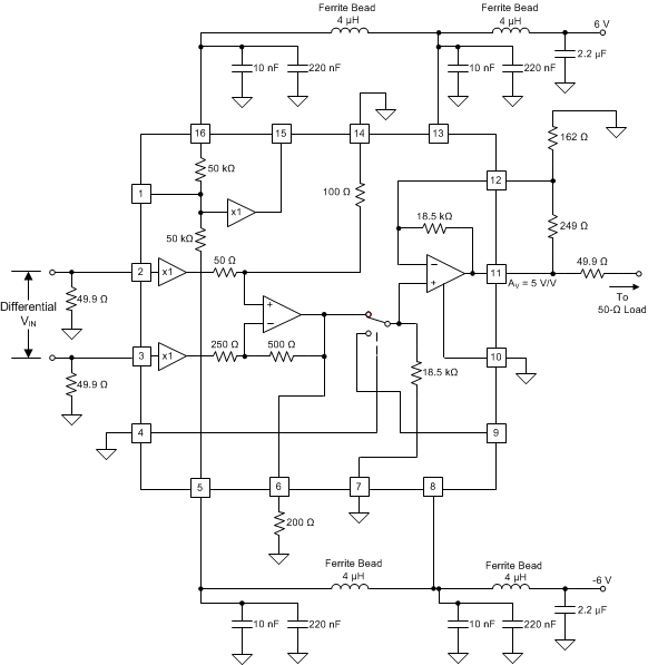
The THS3215 typically operates on balanced, split supplies. The specifications and characterization plots use ±6 V in most cases. The full operating range for the THS3215 spans ±4 V to ±7.9 V. The input and output stages have separate supply pins that are isolated internally.
The recommended external supply configuration brings ±VCC into the output stage first, then back to the input stage connections through a π-filter comprised of ferrite beads and added decoupling capacitors at +VCC2 (pin 16) and –VCC2 (pin 5). Figure 10-1 shows an example decoupling configuration. This same circuit configuration was used to characterize the D2S + OPS performance in Figure 6-1 to Figure 6-12.
 Figure 10-1 Recommended Power-Supply Configuration
The ferrite bead acts to break the feedback loop from the output stage load currents that re-enter the D2S and midscale buffer stages. Operate the two positive supply pins and the two negative supply pins at the same voltage. Using separate sources on the two pins risks forward-biasing the on-chip parallel diodes that connect the two supply inputs together. +VCC1 (pin 13) and +VCC2 (pin 16) have two parallel diodes that are off if the voltage at the two pins are equal. The same is true for –VCC1 (pin 8) and –VCC2 (pin 5).
The THS3215 provides considerable flexibility in the supply voltage settings. The overriding consideration is always satisfying the required headroom to the supplies on all the I/O paths. The logic controls on PATHSEL (pin 4) and DISABLE (pin 10) are intended to operate ground referenced regardless of supplies used. The ground connection on pin 7 is used to set the reference.
Power savings are certainly possible by operating with only the minimum required supplies for the intended swings at each of the pins. For instance, consider an example design operating with a current-sinking DAC with the input common-mode voltage at 3 V, with an output swing at the D2S output of ±1 V. Looking at just the D2S under these conditions, the minimum positive supply is 3 VCM + the maximum input headroom of 1.5 V to the positive supply + the input signal swing of 0.25 V, resulting in a minimum 4.75 V supply for this operation. The ±1 V output at VO1 (pin 6) along with the D2S output headroom sets the minimum negative supply voltage. The maximum 1.5 V headroom gives a possible minimum negative supply of –2.75 V. However, the minimum operating total of 8 V increases the negative supply to –3.5 V.
If the ±1 V swing is then amplified by the OPS, the output swing and headroom requirements set the minimum operating supply. For instance, if the OPS is operating at a gain of 2.5 V/V, the ±2.5 V output requires a maximum headroom of 1.6 V to either supply. Achieving a 1.6 V headroom requires a minimum balanced supply of ±4.1 V. However, the input stage overrides the positive side because the required minimum is 4.75 V, while the negative increases to –4.1 V. This example of absolute minimum supplies saves power. Using a typical 35-mA quiescent current for all stages, going to the minimum 8.5 V total across the device, uses 310 mW of quiescent power versus the 420 mW if a simple ±6 V supply is applied. However, ac performance degrades with the lower headroom. For more power-sensitive applications, consider adjusting the supplies to the minimum required on each side.