SBOS780C March 2016 – June 2021 THS3215
PRODUCTION DATA
- 1 Features
- 2 Applications
- 3 Description
- 4 Revision History
- 5 Pin Configuration and Functions
-
6 Specifications
- 6.1 Absolute Maximum Ratings
- 6.2 ESD Ratings
- 6.3 Recommended Operating Conditions
- 6.4 Thermal Information
- 6.5 Electrical Characteristics: D2S
- 6.6 Electrical Characteristics: OPS
- 6.7 Electrical Characteristics: D2S + OPS
- 6.8 Electrical Characteristics: Midscale (DC) Reference Buffer
- 6.9 Typical Characteristics: D2S + OPS
- 6.10 Typical Characteristics: D2S Only
- 6.11 Typical Characteristics: OPS Only
- 6.12 Typical Characteristics: Midscale (DC) Reference Buffer
- 6.13 Typical Characteristics: Switching Performance
- 6.14 Typical Characteristics: Gain Drift
- 7 Parameter Measurement Information
-
8 Detailed Description
- 8.1 Overview
- 8.2 Functional Block Diagram
- 8.3 Feature Description
- 8.4 Device Functional Modes
-
9 Application and Implementation
- 9.1
Application Information
- 9.1.1
Typical Applications
- 9.1.1.1 High-Frequency, High-Voltage, Dual-Output Line Driver for AWGs
- 9.1.1.2 High-Voltage Pulse-Generator
- 9.1.1.3 Single-Supply, AC-Coupled, Piezo Element Driver
- 9.1.1.4 Output Common-Mode Control Using the Midscale Buffer as a Level Shifter
- 9.1.1.5 Differential I/O Driver With independent Common-Mode Control
- 9.1.1
Typical Applications
- 9.1
Application Information
- 10Power Supply Recommendations
- 11Layout
- 12Device and Documentation Support
- 13Mechanical, Packaging, and Orderable Information
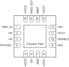
5 Pin Configuration and Functions
 Figure 5-1 RGV Package16-Pin VQFNTop View
Table 5-1 Pin Functions
| PIN | I/O | DESCRIPTION | |
|---|---|---|---|
| NO. | NAME | ||
| 1 | VMID_IN | Input | DC reference buffer input |
| 2 | +IN | Input | Positive signal input to D2S |
| 3 | –IN | Input | Negative signal input to D2S |
| 4 | PATHSEL | Input | Internal SPDT switch control: low selects the internal path, and high selects the external path |
| 5 | –VCC2(1) | Power | Negative supply for input stage |
| 6 | VO1 | Output | D2S external output |
| 7 | GND | Power | Ground for control pins reference |
| 8 | –VCC1(1) | Power | Negative supply for output stage |
| 9 | VIN+ | Input | External OPS noninverting input |
| 10 | DISABLE | Input | Output power stage shutdown control: low enables the OPS, and high disables the OPS |
| 11 | VOUT | Output | OPS output |
| 12 | VIN– | Input | OPS inverting input |
| 13 | +VCC1(1) | Power | Positive supply for output stage |
| 14 | VREF | Input | DC offsetting input to D2S |
| 15 | VMID_OUT | Output | DC reference buffer output |
| 16 | +VCC2(1) | Power | Positive supply for input stage |
| Thermal Pad | — | Connect the thermal pad to GND for single-supply and split-supply operation. See Section 10.1 section for more information. | |
(1) Throughout this document +VCC refers to the voltage
applied at the +VCC1 and +VCC2 pins, and –VCC is the voltage applied
at the –VCC1 and –VCC2 pins.