SBOS780C March 2016 – June 2021 THS3215
PRODUCTION DATA
- 1 Features
- 2 Applications
- 3 Description
- 4 Revision History
- 5 Pin Configuration and Functions
-
6 Specifications
- 6.1 Absolute Maximum Ratings
- 6.2 ESD Ratings
- 6.3 Recommended Operating Conditions
- 6.4 Thermal Information
- 6.5 Electrical Characteristics: D2S
- 6.6 Electrical Characteristics: OPS
- 6.7 Electrical Characteristics: D2S + OPS
- 6.8 Electrical Characteristics: Midscale (DC) Reference Buffer
- 6.9 Typical Characteristics: D2S + OPS
- 6.10 Typical Characteristics: D2S Only
- 6.11 Typical Characteristics: OPS Only
- 6.12 Typical Characteristics: Midscale (DC) Reference Buffer
- 6.13 Typical Characteristics: Switching Performance
- 6.14 Typical Characteristics: Gain Drift
- 7 Parameter Measurement Information
-
8 Detailed Description
- 8.1 Overview
- 8.2 Functional Block Diagram
- 8.3 Feature Description
- 8.4 Device Functional Modes
-
9 Application and Implementation
- 9.1
Application Information
- 9.1.1
Typical Applications
- 9.1.1.1 High-Frequency, High-Voltage, Dual-Output Line Driver for AWGs
- 9.1.1.2 High-Voltage Pulse-Generator
- 9.1.1.3 Single-Supply, AC-Coupled, Piezo Element Driver
- 9.1.1.4 Output Common-Mode Control Using the Midscale Buffer as a Level Shifter
- 9.1.1.5 Differential I/O Driver With independent Common-Mode Control
- 9.1.1
Typical Applications
- 9.1
Application Information
- 10Power Supply Recommendations
- 11Layout
- 12Device and Documentation Support
- 13Mechanical, Packaging, and Orderable Information
8.4.1.2 Internal Connection With Adjustable Common-Mode Output Voltage
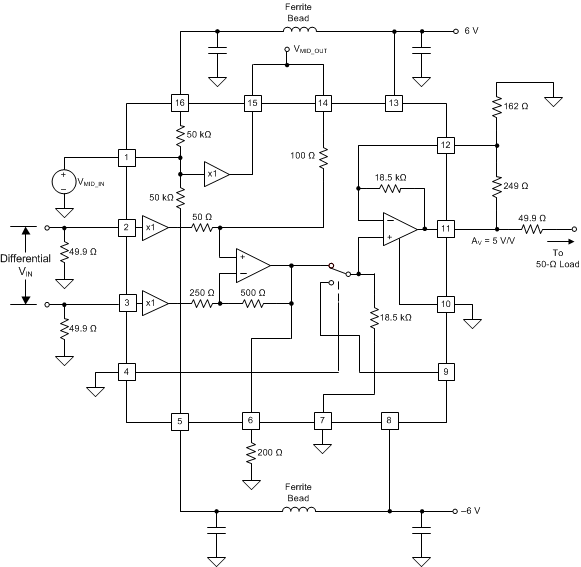
The simplest modification to this starting configuration is using the midscale buffer to drive the VREF pin with either a dc or ac source into VMID_IN (pin 1), shown in Figure 8-16.
 Figure 8-16 Differential to Single-Ended, Gain of 5 V/V Configuration With VREF Driven by
the Midscale Buffer
Figure 8-16 Differential to Single-Ended, Gain of 5 V/V Configuration With VREF Driven by
the Midscale BufferThe VREF input is used to offset the output of the D2S that is then amplified by the OPS. Correct the total dc offset at the output of the OPS by adjusting the voltage at VMID_IN (pin 1). Use the on-chip midscale buffer as a low-impedance source to drive the correction voltage to the VREF pin. A wideband small-signal source can also be summed into this path with a gain of 1 V/V to the D2S output pin. Figure 6-49 shows the midscale buffer to have an extremely flat response through 100 MHz for < 100 mVPPswings, while 1 VPP is supported through 20 MHz with a flat response.
From this point on, the diagrams are simplified to not show the power-supply elements. However, the supplies are required by any application, as described in the Section 9 section.