SBOS780C March 2016 – June 2021 THS3215
PRODUCTION DATA
- 1 Features
- 2 Applications
- 3 Description
- 4 Revision History
- 5 Pin Configuration and Functions
-
6 Specifications
- 6.1 Absolute Maximum Ratings
- 6.2 ESD Ratings
- 6.3 Recommended Operating Conditions
- 6.4 Thermal Information
- 6.5 Electrical Characteristics: D2S
- 6.6 Electrical Characteristics: OPS
- 6.7 Electrical Characteristics: D2S + OPS
- 6.8 Electrical Characteristics: Midscale (DC) Reference Buffer
- 6.9 Typical Characteristics: D2S + OPS
- 6.10 Typical Characteristics: D2S Only
- 6.11 Typical Characteristics: OPS Only
- 6.12 Typical Characteristics: Midscale (DC) Reference Buffer
- 6.13 Typical Characteristics: Switching Performance
- 6.14 Typical Characteristics: Gain Drift
- 7 Parameter Measurement Information
-
8 Detailed Description
- 8.1 Overview
- 8.2 Functional Block Diagram
- 8.3 Feature Description
- 8.4 Device Functional Modes
-
9 Application and Implementation
- 9.1
Application Information
- 9.1.1
Typical Applications
- 9.1.1.1 High-Frequency, High-Voltage, Dual-Output Line Driver for AWGs
- 9.1.1.2 High-Voltage Pulse-Generator
- 9.1.1.3 Single-Supply, AC-Coupled, Piezo Element Driver
- 9.1.1.4 Output Common-Mode Control Using the Midscale Buffer as a Level Shifter
- 9.1.1.5 Differential I/O Driver With independent Common-Mode Control
- 9.1.1
Typical Applications
- 9.1
Application Information
- 10Power Supply Recommendations
- 11Layout
- 12Device and Documentation Support
- 13Mechanical, Packaging, and Orderable Information
8.3.4 Digital Control Lines
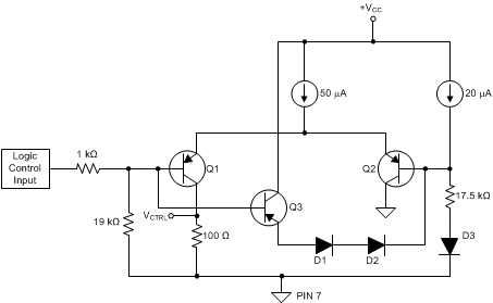
The THS3215 provides two logic input lines that control the input path to the OPS and the OPS power disable feature; both are referenced to GND (pin 7). The control logic defaults to a logic-low state when the pins are externally floated. The GND pin must have a dc path to some reference voltage for correct operation. Float the two logic control lines to enable the OPS and select the internal path connecting the D2S internal output to the OPS noninverting input. Figure 8-14 shows a simplified internal schematic for either logic control input pin.
 Figure 8-14 Logic Control Internal Schematic
The Q2 branch of the differential pair sets up a
switch threshold approximately 1 V greater than
the voltage applied to the GND pin. If the control
input is floating or < 0.7 V, the
differential-pair tail current diverts to the
100-Ω detector load,
and results in an output voltage
(VCTRL, shown in Figure 8-14) that activates the desired mode. The floated
pin default voltage is the PNP base current into
the 19 kΩ resistor. As the control pin voltage
rises above 1.3 V, the differential-pair current
is completely diverted away from the 100 Ω side,
thus switching states.
This unique design allows the logic control inputs to be connected to a single-supply as high as 15.9 V, in order to hold the inputs permanently high, while still accepting a low ground-referenced logic swing for single-supply operation. The NPN transistor (Q3) and two diodes (D1 and D2) act as a clamp to prevent large voltages from appearing across the differential stage.
When the OPS is disabled, both input paths to the OPS are also opened up regardless of the state of PATHSEL (pin 4).