SBOS780C March 2016 – June 2021 THS3215
PRODUCTION DATA
- 1 Features
- 2 Applications
- 3 Description
- 4 Revision History
- 5 Pin Configuration and Functions
-
6 Specifications
- 6.1 Absolute Maximum Ratings
- 6.2 ESD Ratings
- 6.3 Recommended Operating Conditions
- 6.4 Thermal Information
- 6.5 Electrical Characteristics: D2S
- 6.6 Electrical Characteristics: OPS
- 6.7 Electrical Characteristics: D2S + OPS
- 6.8 Electrical Characteristics: Midscale (DC) Reference Buffer
- 6.9 Typical Characteristics: D2S + OPS
- 6.10 Typical Characteristics: D2S Only
- 6.11 Typical Characteristics: OPS Only
- 6.12 Typical Characteristics: Midscale (DC) Reference Buffer
- 6.13 Typical Characteristics: Switching Performance
- 6.14 Typical Characteristics: Gain Drift
- 7 Parameter Measurement Information
-
8 Detailed Description
- 8.1 Overview
- 8.2 Functional Block Diagram
- 8.3 Feature Description
- 8.4 Device Functional Modes
-
9 Application and Implementation
- 9.1
Application Information
- 9.1.1
Typical Applications
- 9.1.1.1 High-Frequency, High-Voltage, Dual-Output Line Driver for AWGs
- 9.1.1.2 High-Voltage Pulse-Generator
- 9.1.1.3 Single-Supply, AC-Coupled, Piezo Element Driver
- 9.1.1.4 Output Common-Mode Control Using the Midscale Buffer as a Level Shifter
- 9.1.1.5 Differential I/O Driver With independent Common-Mode Control
- 9.1.1
Typical Applications
- 9.1
Application Information
- 10Power Supply Recommendations
- 11Layout
- 12Device and Documentation Support
- 13Mechanical, Packaging, and Orderable Information
7.7 Feedthrough Measurement
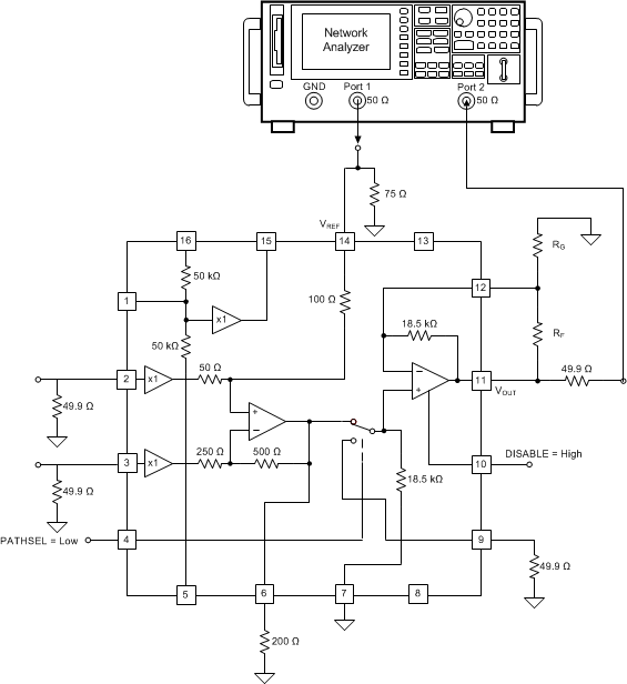
In order to test the forward-feedthrough performance of the OPS in the disabled state, the circuit shown in Figure 7-7 was used. The PATHSEL pin was driven low to select the internal path between the D2S and OPS. A 100 mVPP, swept-frequency, sinusoidal signal was applied at the VREF pin, and the output signal was measured at the OPS output pin (VOUT, pin 11). The transfer function from VREF to the output of the D2S at VO1 has a gain of 0 dB, as shown in Figure 6-23. The results shown in Figure 6-57 account for the 6 dB loss due to the doubly-terminated OPS output, and report the forward feedthrough between VOUT and VO1 at different OPS gains. The D2S inputs were grounded through 50 Ω resistors for this test.
 Figure 7-7 Forward-Feedthrough Test Circuit
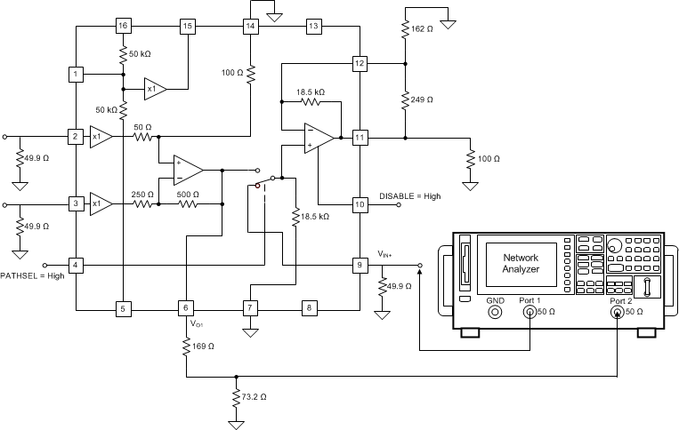
In order to test the reverse feedthrough performance of the OPS in its disabled state, the circuit shown in Figure 7-8 was used. The PATHSEL pin was driven high to select the external path to the OPS noninverting pin, VIN+, pin 9. A 100 mVPP, swept-frequency, sinusoidal signal was applied at the VIN+ pin and the output signal was measured at the D2S output pin (VO1, pin 6). The results shown in Figure 6-58 account for the 16.5 dB loss due to the D2S termination, and the test reports the reverse feedthrough between the VO1 and VIN+ pins. The D2S inputs were grounded through 50 Ω resistors for this test.
 Figure 7-8 Reverse-Feedthrough Test Circuit