SBOS780C March 2016 – June 2021 THS3215
PRODUCTION DATA
- 1 Features
- 2 Applications
- 3 Description
- 4 Revision History
- 5 Pin Configuration and Functions
-
6 Specifications
- 6.1 Absolute Maximum Ratings
- 6.2 ESD Ratings
- 6.3 Recommended Operating Conditions
- 6.4 Thermal Information
- 6.5 Electrical Characteristics: D2S
- 6.6 Electrical Characteristics: OPS
- 6.7 Electrical Characteristics: D2S + OPS
- 6.8 Electrical Characteristics: Midscale (DC) Reference Buffer
- 6.9 Typical Characteristics: D2S + OPS
- 6.10 Typical Characteristics: D2S Only
- 6.11 Typical Characteristics: OPS Only
- 6.12 Typical Characteristics: Midscale (DC) Reference Buffer
- 6.13 Typical Characteristics: Switching Performance
- 6.14 Typical Characteristics: Gain Drift
- 7 Parameter Measurement Information
-
8 Detailed Description
- 8.1 Overview
- 8.2 Functional Block Diagram
- 8.3 Feature Description
- 8.4 Device Functional Modes
-
9 Application and Implementation
- 9.1
Application Information
- 9.1.1
Typical Applications
- 9.1.1.1 High-Frequency, High-Voltage, Dual-Output Line Driver for AWGs
- 9.1.1.2 High-Voltage Pulse-Generator
- 9.1.1.3 Single-Supply, AC-Coupled, Piezo Element Driver
- 9.1.1.4 Output Common-Mode Control Using the Midscale Buffer as a Level Shifter
- 9.1.1.5 Differential I/O Driver With independent Common-Mode Control
- 9.1.1
Typical Applications
- 9.1
Application Information
- 10Power Supply Recommendations
- 11Layout
- 12Device and Documentation Support
- 13Mechanical, Packaging, and Orderable Information
7.2 Frequency Response Measurement
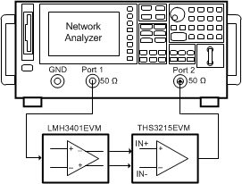
For D2S and full-signal path (D2S + OPS) characterization, the LMH3401, a very wideband, dc-coupled, single-ended to differential amplifier, was used. The LMH3401EVM was used as an interface between a single-ended source and the differential input required by the D2S, shown in Figure 7-2. The LMH3401 provides an input impedance of 50 Ω, and converts a single-ended input to a differential output driving through 50 Ω outputs on each side to what is a 50 Ω termination at each input of the THS3215 D2S.
 Figure 7-2 Frequency-Response Measurement: D2S and Full-Path (D2S + OPS) Circuit
Configurations
Figure 7-2 Frequency-Response Measurement: D2S and Full-Path (D2S + OPS) Circuit
ConfigurationsThe LMH3401 provides 7 GHz bandwidth with 0.1-dB flatness through 700 MHz. From the single-ended matched input (using active match through an internal 12.5 Ω resistor), the LMH3401 produces a differential output with 16-dB gain to the internal output pins. Building out to a 50 Ω source by adding external 40.2 Ω resistors on both differential outputs in series with the internal 10 Ω resistor, results in a net gain of 10 dB to the matched 50 Ω load on the THS3215EVM.
The maximum output swing test for the D2S is 4 VPP (see Figure 6-15 and Figure 6-16). With a fixed gain of 2 V/V, the tests in Figure 6-15 and Figure 6-16 require a 2 VPP differential input. In order to achieve the 2 VPP differential swing at the D2S inputs, the LMH3401 internal outputs must drive a 4 VPP differential signal around the VOCM of the LMH3401. This LMH3401 single-to-differential preamplifier is normally operated with ±2.5 V supplies, and VOCM set to ground. Under these conditions, the LMH3401 supports ±1.4 V on each internal output pin; well beyond the maximum required for THS3215 D2S characterization of ±1 V.
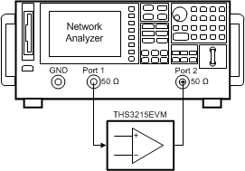
The output of the LMH3401EVM connects directly to the Vin+ (J1) and Vin– (J2) SMA connectors on the THS3215EVM, as shown in Figure 7-1. The physical spacing of the SMA connectors lines up for a direct (no cabling) connection between the two different EVMs using SMA barrels. For THS3215 designs that must be evaluated before any DAC connection, consider using the LMH3401EVM as a gain of 10 dB, single-to-differential interface to the inputs of the D2S. This setup allows single-ended sources to generate differential output signals through the combined LMH3401EVM to THS3215EVM configuration. The D2S, small-signal, frequency-response curves over input common-mode voltage (see Figure 6-13) were generated by adjusting the LMH3401 voltage supplies and maintaining VOCM at midsupply to preserve input headroom on the LMH3401. In order to make single-ended, frequency-response measurements, the configuration shown in Figure 7-3 was used.
 Figure 7-3 Frequency-Response
Measurement: OPS Inverting and Noninverting, Midscale Buffer, and VREF-Input
Circuit Configurations