SBOS780C March 2016 – June 2021 THS3215
PRODUCTION DATA
- 1 Features
- 2 Applications
- 3 Description
- 4 Revision History
- 5 Pin Configuration and Functions
-
6 Specifications
- 6.1 Absolute Maximum Ratings
- 6.2 ESD Ratings
- 6.3 Recommended Operating Conditions
- 6.4 Thermal Information
- 6.5 Electrical Characteristics: D2S
- 6.6 Electrical Characteristics: OPS
- 6.7 Electrical Characteristics: D2S + OPS
- 6.8 Electrical Characteristics: Midscale (DC) Reference Buffer
- 6.9 Typical Characteristics: D2S + OPS
- 6.10 Typical Characteristics: D2S Only
- 6.11 Typical Characteristics: OPS Only
- 6.12 Typical Characteristics: Midscale (DC) Reference Buffer
- 6.13 Typical Characteristics: Switching Performance
- 6.14 Typical Characteristics: Gain Drift
- 7 Parameter Measurement Information
-
8 Detailed Description
- 8.1 Overview
- 8.2 Functional Block Diagram
- 8.3 Feature Description
- 8.4 Device Functional Modes
-
9 Application and Implementation
- 9.1
Application Information
- 9.1.1
Typical Applications
- 9.1.1.1 High-Frequency, High-Voltage, Dual-Output Line Driver for AWGs
- 9.1.1.2 High-Voltage Pulse-Generator
- 9.1.1.3 Single-Supply, AC-Coupled, Piezo Element Driver
- 9.1.1.4 Output Common-Mode Control Using the Midscale Buffer as a Level Shifter
- 9.1.1.5 Differential I/O Driver With independent Common-Mode Control
- 9.1.1
Typical Applications
- 9.1
Application Information
- 10Power Supply Recommendations
- 11Layout
- 12Device and Documentation Support
- 13Mechanical, Packaging, and Orderable Information
8.3.2 Midscale (DC) Reference Buffer (Pin 1 and Pin 15)
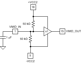
This optional block can be completely unconnected and not used if the design does not require this feature. Internal 50 kΩ resistors to the power supplies bias the input of the buffer to the midpoint of the supplies used. The internal resistors set a midsupply operating point when the buffer is not used, as well as a default midsupply point at the buffer output to be used in other stages for single-supply, ac-coupled applications.
The buffer provides a very wideband, low output-impedance when used to drive VREF, pin 14 (see Figure 6-51). To provide this low broadband impedance, the closed-loop midscale (dc) reference buffer offers a very broadband SSBW, but only a modest large-signal bandwidth (LSBW); see Figure 6-49. This path is not normally intended to inject a wideband signal, but can be used for lower-amplitude signals. Driving the buffer output into the VREF pin allows a wideband small-signal term to be added into the D2S along with the signal from the differential inputs.
The midscale (or dc) reference buffer injects an offset voltage to the output offset of the D2S when it drives the VREF pin. The offset has very low drift, but consider the effect of the input bias current times the dc source impedance at VMID_IN (pin 1). When used as a default midsupply reference for single-supply operation, the input to this buffer is just the average of the total power supplies though a 25 kΩ source impedance. Add an external capacitor to filter the supply and the 50 kΩ internal resistors. A 1-µF capacitor on VMID_IN adds a 6-Hz pole to the noise sources. If lower noise at lower frequencies is required, implement a midscale divider with external, lower-valued resistors in parallel with the internal 50 kΩ values.
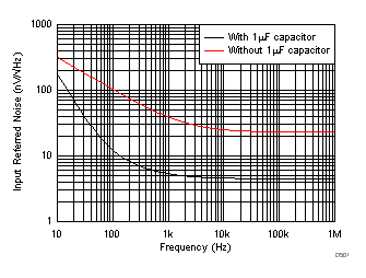
If the midscale buffer drives the VREF pin, the buffer noise is added to Equation 9 and Equation 10. The midscale buffer 4.4 nV/√ Hz voltage noise is amplified by 0 dB, and adds (RMS) a negligible impact to the total D2S output noise. The biggest impact comes when the internal default 50 kΩ dividers are used. Be sure to decouple VMID_IN with at least a 1 µF capacitor in the application to reduce the noise contribution through this path. Figure 8-5 shows the simulation circuit with the 1 µF capacitor installed. Figure 8-6 shows the simulated output noise for the midscale buffer using the internal 50 kΩ divider with and without the 1 µF capacitor on VMID_IN.
 Figure 8-5 Midscale
Buffer Noise Model
 Figure 8-6 Buffer-Output Noise Comparison With and Without the 1 µF Bypass Capacitor on
VMID_IN
Figure 8-6 Buffer-Output Noise Comparison With and Without the 1 µF Bypass Capacitor on
VMID_INIn the flat region, the 1 µF capacitor reduces the midscale buffer output spot noise from approximately 55 nV/√ Hz to 4.4 nV/√ Hz. If the noise below 100 Hz is unacceptable, either add a low-noise buffer to drive this input, or add lower-value resistors externally to set up the midsupply bias. Also, consider the noise impact of any reference voltage source driving the midscale buffer path.