SBOS859B March 2018 – July 2018 INA1620
PRODUCTION DATA.
- 1 Features
- 2 Applications
- 3 Description
- 4 Revision History
- 5 Pin Configuration and Functions
- 6 Specifications
- 7 Detailed Description
- 8 Application and Implementation
- 9 Power Supply Recommendations
- 10Layout
- 11Device and Documentation Support
- 12Mechanical, Packaging, and Orderable Information
7.3.1 Matched Thin-Film Resistor Pairs
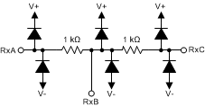
The INA1620 integrates four thin-film resistor pairs. Each pair is made up of two thin-film resistors with a nominal resistance of 1 kΩ. While the absolute value of the resistor is not trimmed and can vary significantly, the two resistors in an pair are designed to match each other extremely well. The resistors in an pair typically match to within 0.004% of each other's value. This matching is also preserved well over temperature, with the matching drift having a 0.2 ppm/°C maximum specification. Each node in the resistor pair is bonded out to a pad on the INA1620 package allowing the resistor pairs to be used in multiple configurations. The nodes in the pair are protected from damage due to electrostatic discharge (ESD) events by diodes tied to the power supplies of the IC. For this reason, voltages beyond the power supplies cannot be applied to the resistors without forward-biasing the ESD protection diodes. The resistor pairs should not be used if there is no power applied to the INA1620. The configuration of the ESD protection diodes is shown in Figure 44.
 Figure 44. ESD Protection Diodes on Each Resistor Pair
 Although the resistor pairs and amplifier core are fabricated on the same silicon substrate, they can be used in separate circuits as long as the previously-mentioned voltage limits are observed. The functional state of the amplifier (enabled or shutdown) does not affect the resistor pair's performance.