SBOS923I December   2017  – July 2024 LMV321A , LMV324A , LMV358A

PRODUCTION DATA  

  1.   1
  2. Features
  3. Applications
  4. Description
  5. Pin Functions and Configurations
  6. Specifications
    1. 5.1 Absolute Maximum Ratings
    2. 5.2 ESD Ratings
    3. 5.3 Recommended Operating Conditions
    4. 5.4 Thermal Information: LMV321A
    5. 5.5 Thermal Information: LMV358A
    6. 5.6 Thermal Information: LMV324A
    7. 5.7 Electrical Characteristics
    8. 5.8 Typical Characteristics
  7. Detailed Description
    1. 6.1 Overview
    2. 6.2 Functional Block Diagram
    3. 6.3 Feature Description
      1. 6.3.1 Operating Voltage
      2. 6.3.2 Input Common Mode Range
      3. 6.3.3 Rail-to-Rail Output
      4. 6.3.4 Overload Recovery
    4. 6.4 Device Functional Modes
  8. Application and Implementation
    1. 7.1 Application Information
    2. 7.2 Typical Application
      1. 7.2.1 LMV3xxA Low-Side, Current Sensing Application
        1. 7.2.1.1 Design Requirements
        2. 7.2.1.2 Detailed Design Procedure
        3. 7.2.1.3 Application Curve
      2. 7.2.2 Single-Supply Photodiode Amplifier
        1. 7.2.2.1 Design Requirements
        2. 7.2.2.2 Detailed Design Procedure
        3. 7.2.2.3 Application Curves
    3. 7.3 Power Supply Recommendations
      1. 7.3.1 Input and ESD Protection
    4. 7.4 Layout
      1. 7.4.1 Layout Guidelines
      2. 7.4.2 Layout Example
  9. Device and Documentation Support
    1. 8.1 Documentation Support
      1. 8.1.1 Related Documentation
    2. 8.2 Receiving Notification of Documentation Updates
    3. 8.3 Support Resources
    4. 8.4 Trademarks
    5. 8.5 Electrostatic Discharge Caution
    6. 8.6 Glossary
  10. Revision History
  11. 10Mechanical, Packaging, and Orderable Information

LMV3xxA Low-Side, Current Sensing Application

Figure 7-1 shows the LMV3xxA configured in a low-side current sensing application.
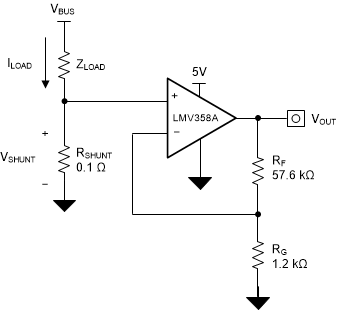
LMV321A LMV358A LMV324A LMV3xxA in a Low-Side, Current-Sensing ApplicationFigure 7-1 LMV3xxA in a Low-Side, Current-Sensing Application