SBOS926H January 2021 – November 2024 OPA2392 , OPA392
PRODMIX
- 1
- 1 Features
- 2 Applications
- 3 Description
- 4 Device Comparison Table
- 5 Pin Configuration and Functions
- 6 Specifications
- 7 Detailed Description
- 8 Application and Implementation
- 9 Device and Documentation Support
- 10Revision History
- 11Mechanical, Packaging, and Orderable Information
5 Pin Configuration and Functions
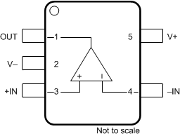
 Figure 5-1 OPA392 DBV Package, 5-Pin SOT-23 (Top View)
Figure 5-3 OPA392 YBJ Package, 6-Pin DSBGA (Top View)
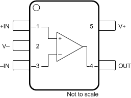
 Figure 5-2 OPA392 DCK Package, 5-Pin SC70 (Top View)
Table 5-1 Pin Functions: OPA392
| PIN | TYPE | DESCRIPTION | |||
|---|---|---|---|---|---|
| NAME | NO. | ||||
| DBV (SOT-23) | DCK (SC70) | YBJ (DSBGA) | |||
| EN | — | — | B2 | Input | Enable pin. High = amplifier enabled. |
| –IN | 4 | 3 | B1 | Input | Inverting input |
| +IN | 3 | 1 | C1 | Input | Noninverting input |
| OUT | 1 | 4 | A1 | Output | Output |
| V– | 2 | 2 | C2 | Power | Negative (lowest) power supply |
| V+ | 5 | 5 | A2 | Power | Positive (highest) power supply |
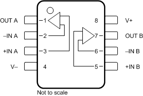
 Figure 5-4 OPA2392 D Package, 8-Pin SOIC and DGK Package, 8-Pin VSSOP (Top
View)
Figure 5-4 OPA2392 D Package, 8-Pin SOIC and DGK Package, 8-Pin VSSOP (Top
View)Figure 5-6 OPA2392 YBJ Package, 9-Pin DSBGA (Top View)
Figure 5-5 OPA2392 DSG Package, 8-Pin WSON With Exposed Thermal Pad (Top
View)
Table 5-2 Pin Functions: OPA2392
| PIN | TYPE | DESCRIPTION | |||
|---|---|---|---|---|---|
| NAME | NO. | ||||
| D (SOIC), DGK (VSSOP) |
DSG (WSON) | YBJ (DSBGA) | |||
| EN | — | — | B2 | Input | Enable pin. High = both amplifiers enabled. |
| –IN A | 2 | 2 | B1 | Input | Inverting input, channel A |
| +IN A | 3 | 3 | C1 | Input | Noninverting input, channel A |
| –IN B | 6 | 6 | B3 | Input | Inverting input, channel B |
| +IN B | 5 | 5 | C3 | Input | Noninverting input, channel B |
| OUT A | 1 | 1 | A1 | Output | Output, channel A |
| OUT B | 7 | 7 | A3 | Output | Output, channel B |
| V– | 4 | 4 | C2 | Power | Negative (lowest) power supply |
| V+ | 8 | 8 | A2 | Power | Positive (highest) power supply |
| Thermal Pad | — | Thermal pad | — | — | Connect thermal pad to V– |
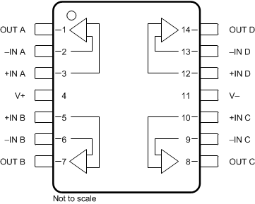
 Figure 5-7 OPA4392 PW Preview Package, 14-Pin TSSOP (Top View)
Figure 5-8 OPA4392 RTE Preview Package, 16-Pin WQFN (Top View)
Table 5-3 Pin Functions: OPA4392
| PIN | TYPE | DESCRIPTION | ||
|---|---|---|---|---|
| NAME | NO. | |||
| PW (TSSOP) | RTE (WQFN) | |||
| EN AB | — | 6 | Input | Enable pin for A and B amplifiers. High = amplifiers A and B are enabled. |
| EN CD | — | 7 | Input | Enable pin for C and D amplifiers. High = amplifiers C and D are enabled. |
| –IN A | 2 | 16 | Input | Inverting input, channel A |
| +IN A | 3 | 1 | Input | Noninverting input, channel A |
| –IN B | 6 | 4 | Input | Inverting input, channel B |
| +IN B | 5 | 3 | Input | Noninverting input, channel B |
| –IN C | 9 | 9 | Input | Inverting input, channel C |
| +IN C | 10 | 10 | Input | Noninverting input, channel C |
| –IN D | 13 | 13 | Input | Inverting input, channel D |
| +IN D | 12 | 12 | Input | Noninverting input, channel D |
| OUT A | 1 | 15 | Output | Output, channel A |
| OUT B | 7 | 5 | Output | Output, channel B |
| OUT C | 8 | 8 | Output | Output, channel C |
| OUT D | 14 | 14 | Output | Output, channel D |
| Thermal Pad | — | Thermal Pad | Power | Connect thermal pad to V– |
| V– | 11 | 11 | Power | Negative (lowest) power supply |
| V+ | 4 | 2 | Power | Positive (highest) power supply |