SBOS932C January 2020 – March 2021 THP210
PRODUCTION DATA
- 1 Features
- 2 Applications
- 3 Description
- 4 Revision History
- 5 Pin Configuration and Functions
- 6 Specifications
- 7 Parameter Measurement Information
- 8 Detailed Description
-
9 Application and Implementation
- 9.1 Application Information
- 9.2 Typical Applications
- 10Power Supply Recommendations
- 11Layout
- 12Device and Documentation Support
- 13Mechanical, Packaging, and Orderable Information
8.3.4 Amplifier Overload Power Limit
During overload or fault conditions, many bipolar-based amplifiers draw significant (three to five times) quiescent current if the output voltage is clipped (meaning the output voltage becomes limited by the negative or positive supply rail).
The primary cause for this condition is that common-emitter output stages can consume excessive base current (up to 100x) when overdriven into saturation. In addition, the overload condition causes the feedback to be broken, which causes the slew boost to be permanently on. Depending on the slew boost circuit, this increases the tail current up to 4x.
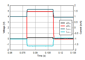
The THP210 has an intelligent overload detection scheme that eliminates this problem, meaning that there is virtually no additional current consumption in the case of an overload event, represented in Figure 8-1. The protection circuit continuously monitors both the input and output stages of the amplifier. Figure 8-1 shows a measurements of the overload power limit behavior. If a large input voltage step (referred to as ΔVIN) is detected, the protection circuit checks for the presence of a rapid change in the voltage at the output (referred to as ΔVO). If the output is not changing because the output is clipped at supply rail, the protection circuit disables the slew-boost circuit and limit the base current of the predriver to prevent output saturation. After the overload condition is removed, the amplifier rapidly recovers to normal operating condition. Figure 8-1 indicates that in case of an overloaded output the current consumption at the supply pins (referred to I(VS+) and I(VS–)) does not exceed the limitations, and quickly recovers as soon as the overload condition has been removed.
 Figure 8-1 Supply Current Change With Overloaded Outputs