SBOSA04D March   2022  – December 2024 INA296A , INA296B

PRODUCTION DATA  

  1.   1
  2. Features
  3. Applications
  4. Description
  5. Device Comparison
  6. Pin Configuration and Functions
  7. Specifications
    1. 6.1 Absolute Maximum Ratings
    2. 6.2 ESD Ratings
    3. 6.3 Recommended Operating Conditions
    4. 6.4 Thermal Information
    5. 6.5 Electrical Characteristics
    6. 6.6 Typical Characteristics
  8. Detailed Description
    1. 7.1 Overview
    2. 7.2 Functional Block Diagram
    3. 7.3 Feature Description
      1. 7.3.1 Amplifier Input Common-Mode Signal
        1. 7.3.1.1 Input-Signal Bandwidth
        2. 7.3.1.2 Low Input Bias Current
        3. 7.3.1.3 Low VSENSE Operation
        4. 7.3.1.4 Wide Fixed Gain Output
        5. 7.3.1.5 Wide Supply Range
    4. 7.4 Device Functional Modes
      1. 7.4.1 Adjusting the Output With the Reference Pins
      2. 7.4.2 Reference Pin Connections for Unidirectional Current Measurements
        1. 7.4.2.1 Ground Referenced Output
        2. 7.4.2.2 VS Referenced Output
      3. 7.4.3 Reference Pin Connections for Bidirectional Current Measurements
        1. 7.4.3.1 Output Set to External Reference Voltage
        2. 7.4.3.2 Output Set to Mid-Supply Voltage
        3. 7.4.3.3 Output Set to Mid-External Reference
        4. 7.4.3.4 Output Set Using Resistor Divider
      4. 7.4.4 High Signal Throughput
  9. Application and Implementation
    1. 8.1 Application Information
      1. 8.1.1 RSENSE and Device Gain Selection
    2. 8.2 Typical Application
      1. 8.2.1 Current Sensing in a Solenoid Application
        1. 8.2.1.1 Design Requirements
        2. 8.2.1.2 Detailed Design Procedure
        3. 8.2.1.3 Application Curve
    3. 8.3 Power Supply Recommendations
      1. 8.3.1 Power Supply Decoupling
    4. 8.4 Layout
      1. 8.4.1 Layout Guidelines
      2. 8.4.2 Layout Examples
  10. Device and Documentation Support
    1. 9.1 Documentation Support
      1. 9.1.1 Related Documentation
    2. 9.2 Receiving Notification of Documentation Updates
    3. 9.3 Support Resources
    4. 9.4 Trademarks
    5. 9.5 Electrostatic Discharge Caution
    6. 9.6 Glossary
  11. 10Revision History
  12. 11Mechanical, Packaging, and Orderable Information

Output Set to External Reference Voltage

Connecting both pins together and then to a reference voltage results in an output voltage equal to the reference voltage for the condition of shorted input pins or a 0V differential input. Figure 7-4 shows this configuration. The output voltage decreases below the reference voltage when the IN+ pin is negative relative to the IN– pin and increases when the IN+ pin is positive relative to the IN– pin. This technique is the most accurate way to bias the output to a precise voltage.
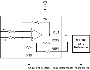
INA296A INA296B External Reference OutputFigure 7-4 External Reference Output