SBOSA42 June 2024 OPA596
ADVANCE INFORMATION
- 1
- 1 Features
- 2 Applications
- 3 Description
- 4 Pin Configuration and Functions
- 5 Specifications
- 6 Detailed Description
-
7 Application and Implementation
- 7.1 Application Information
- 7.2 Typical Applications
- 7.3 Power Supply Recommendations
- 7.4 Layout
- 8 Device and Documentation Support
- 9 Revision History
- 10Mechanical, Packaging, and Orderable Information
4 Pin Configuration and Functions
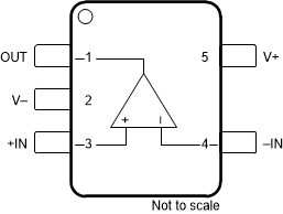
 Figure 4-1 OPA596 DBV Package, 5-Pin
SOT-23 (Top View)
Figure 4-1 OPA596 DBV Package, 5-Pin
SOT-23 (Top View)Table 4-1 Pin Functions: OPA596
| PIN | TYPE | DESCRIPTION | |
|---|---|---|---|
| NAME | NO. | ||
| +IN | 3 | Input | Noninverting input |
| –IN | 4 | Input | Inverting input |
| OUT | 1 | Output | Output |
| V+ | 5 | Power | Positive (highest) power supply |
| V– | 2 | Power | Negative (lowest) power supply |
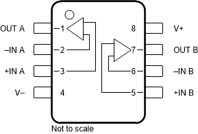
 Figure 4-2 OPA2596 DGK Package, 8-Pin
VSSOP (Top View)
Figure 4-2 OPA2596 DGK Package, 8-Pin
VSSOP (Top View)Table 4-2 Pin Functions: OPA2596
| PIN | TYPE | DESCRIPTION | |
|---|---|---|---|
| NAME | NO. | ||
| +IN A | 3 | Input | Noninverting input, channel A |
| +IN B | 5 | Input | Noninverting input, channel B |
| –IN A | 2 | Input | Inverting input, channel A |
| –IN B | 6 | Input | Inverting input, channel B |
| OUT A | 1 | Output | Output, channel A |
| OUT B | 7 | Output | Output, channel B |
| V+ | 8 | Power | Positive (highest) power supply |
| V– | 4 | Power | Negative (lowest) power supply |