SBOSA95F May 2022 – October 2024 OPA2863A , OPA863A
PRODUCTION DATA
- 1
- 1 Features
- 2 Applications
- 3 Description
- 4 Device Comparison Table
- 5 Pin Configuration and Functions
-
6 Specifications
- 6.1 Absolute Maximum Ratings
- 6.2 ESD Ratings
- 6.3 Recommended Operating Conditions
- 6.4 Thermal Information OPA863A
- 6.5 Thermal Information OPA2863A
- 6.6 Electrical Characteristics VS = ±5 V
- 6.7 Electrical Characteristics VS = 3 V
- 6.8 Typical Characteristics: VS = ±5 V
- 6.9 Typical Characteristics: VS = 3 V
- 6.10 Typical Characteristics: VS = 3 V to 10 V
- 7 Detailed Description
- 8 Application and Implementation
- 9 Device and Documentation Support
- 10Revision History
- 11Mechanical, Packaging, and Orderable Information
5 Pin Configuration and Functions
 Figure 5-1 OPA863A DBV Package, 5-Pin
SOT-23 (Top View)
Figure 5-1 OPA863A DBV Package, 5-Pin
SOT-23 (Top View)Table 5-1 Pin Functions: OPA863A
| PIN | TYPE | DESCRIPTION | |
|---|---|---|---|
| NAME | NO. | ||
| VIN+ | 3 | Input | Noninverting input pin |
| VIN– | 4 | Input | Inverting input pin |
| VOUT | 1 | Output | Output pin |
| VS– | 2 | Power | Negative power-supply pin |
| VS+ | 5 | Power | Positive power-supply pin |
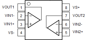
 Figure 5-2 OPA2863A D Package,
 8-Pin SOIC and DGK (Preview) Package,
8-Pin VSSOP (Top View)
 Figure 5-3 OPA2863A DSN Package,
10-Pin USON With Exposed Thermal Pad (Top View)
Figure 5-3 OPA2863A DSN Package,
10-Pin USON With Exposed Thermal Pad (Top View)Table 5-2 Pin Functions:
OPA2863A
| PIN | TYPE | DESCRIPTION | ||
|---|---|---|---|---|
| NAME | NO. | |||
| D (SOIC), DGK (VSSOP) |
DSN (USON) | |||
| PD1 | — | 5 | Input | Amplifier 1 power down. Low = disabled, high = enabled |
| PD2 | — | 6 | Input | Amplifier 2 power down. Low = disabled, high = enabled |
| VIN1– | 2 | 2 | Input | Amplifier 1 inverting input pin |
| VIN1+ | 3 | 3 | Input | Amplifier 1 noninverting input pin |
| VIN2– | 6 | 8 | Input | Amplifier 2 inverting input pin |
| VIN2+ | 5 | 7 | Input | Amplifier 2 noninverting input pin |
| VOUT1 | 1 | 1 | Output | Amplifier 1 output pin |
| VOUT2 | 7 | 9 | Output | Amplifier 2 output pin |
| VS– | 4 | 4 | Power | Negative power-supply pin |
| VS+ | 8 | 10 | Power | Positive power-supply pin |
| Thermal pad | — | Thermal pad | — | Thermal pad. Electrically isolated from the device. Connect to a heat-spreading plane, typically ground. |