SBOSAD7A April   2023  – August 2024 TLV9161-Q1 , TLV9162-Q1 , TLV9164-Q1

PRODUCTION DATA  

  1.   1
  2. Features
  3. Applications
  4. Description
  5. Pin Configuration and Functions
  6. Specifications
    1. 5.1 Absolute Maximum Ratings
    2. 5.2 ESD Ratings
    3. 5.3 Recommended Operating Conditions
    4. 5.4 Thermal Information for Single Channel
    5. 5.5 Thermal Information for Dual Channel
    6. 5.6 Thermal Information for Quad Channel
    7. 5.7 Electrical Characteristics
    8. 5.8 Typical Characteristics
  7. Detailed Description
    1. 6.1 Overview
    2. 6.2 Functional Block Diagram
    3. 6.3 Feature Description
      1. 6.3.1 Input Protection Circuitry
      2. 6.3.2 EMI Rejection
      3. 6.3.3 Thermal Protection
      4. 6.3.4 Capacitive Load and Stability
      5. 6.3.5 Common-Mode Voltage Range
      6. 6.3.6 Phase Reversal Protection
      7. 6.3.7 Electrical Overstress
      8. 6.3.8 Overload Recovery
      9. 6.3.9 Typical Specifications and Distributions
    4. 6.4 Device Functional Modes
  8. Application and Implementation
    1. 7.1 Application Information
    2. 7.2 Typical Applications
      1. 7.2.1 Low-Side Current Measurement
        1. 7.2.1.1 Design Requirements
        2. 7.2.1.2 Detailed Design Procedure
        3. 7.2.1.3 Application Curves
    3. 7.3 Power Supply Recommendations
    4. 7.4 Layout
      1. 7.4.1 Layout Guidelines
      2. 7.4.2 Layout Example
  9. Device and Documentation Support
    1. 8.1 Device Support
      1. 8.1.1 Development Support
        1. 8.1.1.1 TINA-TI (Free Software Download)
    2. 8.2 Documentation Support
      1. 8.2.1 Related Documentation
    3. 8.3 Receiving Notification of Documentation Updates
    4. 8.4 Support Resources
    5. 8.5 Trademarks
    6. 8.6 Electrostatic Discharge Caution
    7. 8.7 Glossary
  10. Revision History
  11. 10Mechanical, Packaging, and Orderable Information

Description

The TLV916x-Q1 family (TLV9161-Q1, TLV9162-Q1, and TLV9164-Q1) is a family of 16V, general-purpose automotive operational amplifiers. These devices offer exceptional DC precision and AC performance, including rail-to-rail input or output, low offset (±210µV, typical), low-offset drift (±0.25µV/°C, typical), and low noise (6.8nV/√Hz at 1kHz, 4.2nV/√Hz at 10kHz).

Features such as wide differential input voltage range, high short-circuit current (±73mA), and high slew rate (33V/µs) make the TLV916x-Q1 a flexible, robust, and high-performance op amp for automotive applications.

The TLV916x-Q1 family of op amps is available in standard packages and is specified from –40°C to 125°C.

Package Information
PART NUMBER(1) CHANNEL COUNT PACKAGE PACKAGE SIZE(2)
TLV9161-Q1 Single DBV (SOT-23, 5) 2.9mm × 2.8mm
DCK (SC70, 5) 2mm × 2.1mm
TLV9162-Q1 Dual D (SOIC, 8) 4.9mm × 6mm
DGK (VSSOP, 8) 3mm × 4.9mm
PW (TSSOP, 8) 3mm × 6.4mm
TLV9164-Q1 Quad D (SOIC, 14) 8.65mm × 6mm
PW (TSSOP, 14) 5mm × 6.4mm
For all available packages, see the orderable addendum at the end of the data sheet.
The package size (length × width) is a nominal value and includes pins, where applicable.
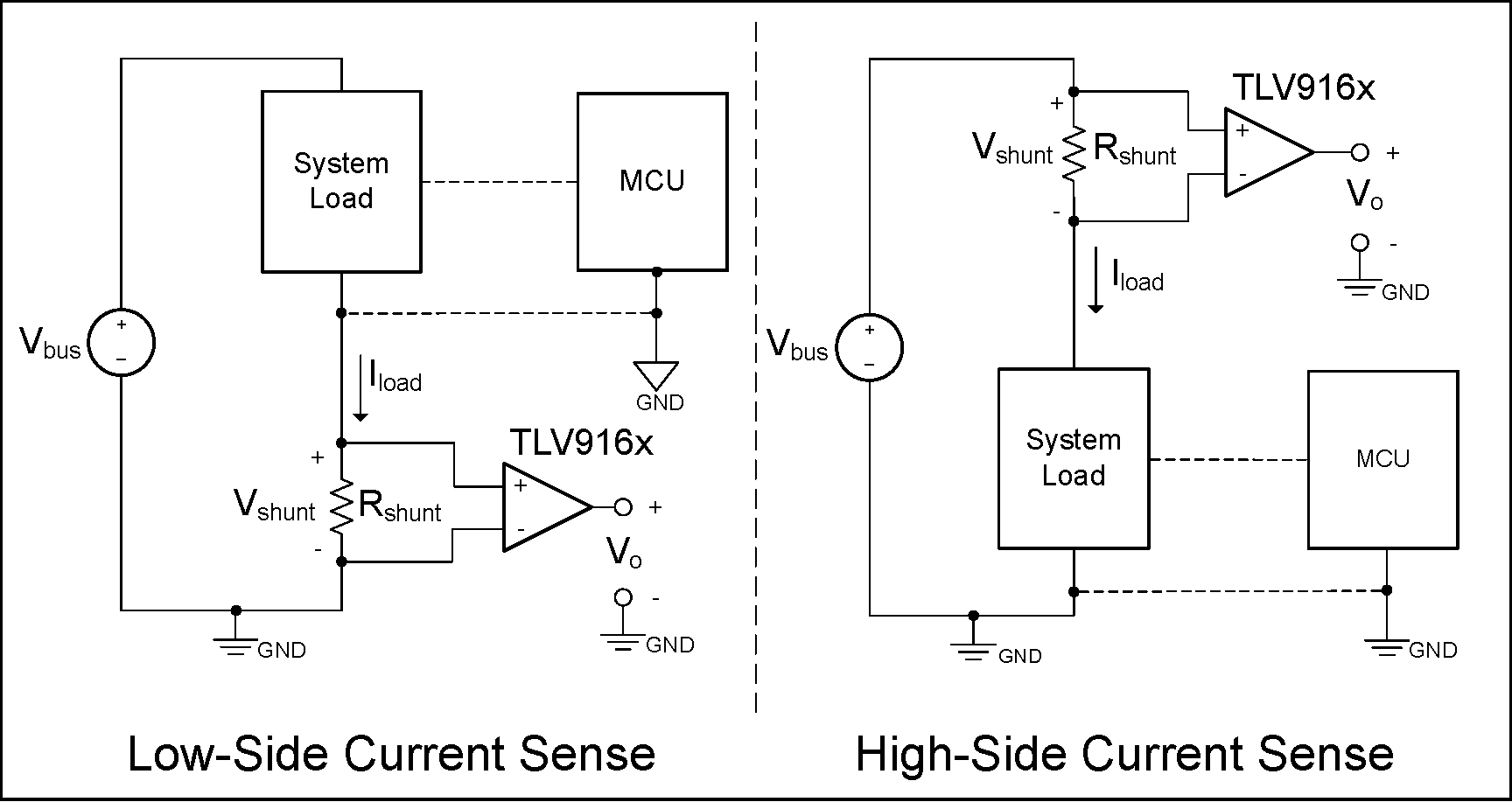
TLV9161-Q1 TLV9162-Q1 TLV9164-Q1 TLV916x-Q1 in Current-Sensing Applications TLV916x-Q1 in Current-Sensing Applications