SBOSAG6B November   2023  – October 2024 OPA2994-Q1 , OPA994-Q1

PRODUCTION DATA  
  1.   1
  2. Features
  3. Applications
  4. Description
  5. Pin Configuration and Functions
  6. Specifications
    1. 5.1 Absolute Maximum Ratings
    2. 5.2 ESD Ratings
    3. 5.3 Recommended Operating Conditions
    4. 5.4 Thermal Information for Single Channel
    5. 5.5 Thermal Information for Dual Channel
    6. 5.6 Electrical Characteristics
    7. 5.7 Typical Characteristics
  7. Detailed Description
    1. 6.1 Overview
    2. 6.2 Functional Block Diagram
    3. 6.3 Feature Description
      1. 6.3.1 Unlimited Capacitive Load Drive
      2. 6.3.2 Common-Mode Voltage Range
      3. 6.3.3 Phase Reversal Protection
      4. 6.3.4 Electrical Overstress
      5. 6.3.5 Overload Recovery
      6. 6.3.6 Typical Specifications and Distributions
    4. 6.4 Device Functional Modes
  8. Application and Implementation
    1. 7.1 Application Information
    2. 7.2 Typical Applications
      1. 7.2.1 Low-Side Current Measurement
        1. 7.2.1.1 Design Requirements
        2. 7.2.1.2 Detailed Design Procedure
        3. 7.2.1.3 Application Curve
    3. 7.3 Power Supply Recommendations
    4. 7.4 Layout
      1. 7.4.1 Layout Guidelines
      2. 7.4.2 Layout Example
  9. Device and Documentation Support
    1. 8.1 Device Support
      1. 8.1.1 Development Support
        1. 8.1.1.1 TINA-TI (Free Software Download)
    2. 8.2 Documentation Support
      1. 8.2.1 Related Documentation
    3. 8.3 Receiving Notification of Documentation Updates
    4. 8.4 Support Resources
    5. 8.5 Trademarks
    6. 8.6 Electrostatic Discharge Caution
    7. 8.7 Glossary
  10. Revision History
  11. 10Mechanical, Packaging, and Orderable Information

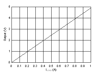
Application Curve

OPA994-Q1 OPA2994-Q1 Low-Side, Current-Sense,
                    Transfer FunctionFigure 7-2 Low-Side, Current-Sense, Transfer Function