SBOU024C august 2004 – july 2023 PGA309
- 1
- Read This First
-
1Introduction
- 1.1 PGA309 Functional Description
- 1.2 Sensor Error Adjustment Range
- 1.3 Gain Scaling
- 1.4 Offset Adjustment
- 1.5 Voltage Reference
- 1.6 Sensor Excitation and Linearization
- 1.7 ADC for Temperature Sensing
- 1.8 External EEPROM and Temperature Coefficients
- 1.9 Fault Monitor
- 1.10 Over-Scale and Under-Scale Limits
- 1.11 Power-Up and Normal Operation
- 1.12 Digital Interface
- 1.13 Pin Configuration
- 2Detailed Description
- 3Operating Modes
-
4Digital Interface
- 4.1 Description
- 4.2 Two-Wire Interface
- 4.3 One-Wire Interface
- 4.4 One-Wire Interface Timeout
- 4.5 One-Wire Interface Timing Considerations
- 4.6 Two-Wire Access to External EEPROM
- 4.7 One-Wire Interface Initiated Two-Wire EEPROM Transactions
- 4.8 PGA309 Stand-Alone Mode and Two-Wire Transactions
- 4.9 PGA309 Two-Wire Bus Master Operation and Bus Sharing Considerations
- 4.10 One-Wire Operation with PRG Connected to VOUT
- 4.11 Four-Wire Modules and One-Wire Interface (PRG)
- 5Application Background
-
6Register Descriptions
- 6.1 Internal Register Overview
- 6.2
Internal Register Map
- 6.2.1 Register 0: Temp ADC Output Register (Read Only, Address Pointer = 00000)
- 6.2.2 Register 1: Fine Offset Adjust (Zero DAC) Register (Read/Write, Address Pointer = 00001)
- 6.2.3 Register 2: Fine Gain Adjust (Gain DAC) Register (Read/Write, Address Pointer = 00010)
- 6.2.4 Register 3: Reference Control and Linearization Register (Read/Write, Address Pointer = 00011)
- 6.2.5 Register 4: PGA Coarse Offset Adjust and Gain Select/Output Amplifier Gain Select Register (Read/Write, Address Pointer = 00100)
- 6.2.6 Register 5: PGA Configuration and Over/Under-Scale Limit Register (Read/Write, Address Pointer = 00101)
- 6.2.7 Register 6: Temp ADC Control Register (Read/Write, Address Pointer = 00110)
- 6.2.8 Register 7: Output Enable Counter Control Register (Read/Write, Address Pointer = 00111)
- 6.2.9 Register 8: Alarm Status Register (Read Only, Address Pointer = 01000)
- A External EEPROM Example
- B Detailed Block Diagram
- C Glossary
- Revision History
2.2 Offset Scaling
The coarse offset adjust is implemented before the Front-End PGA gain to allow for maximum dynamic range. Many bridge sensors have initial offsets comparable to their maximum scale outputs. The coarse offset adjust can be applied as positive or negative. It is implemented in a 4-bit DAC + sign and contains 14 positive selections, 14 negative selections, and zero.
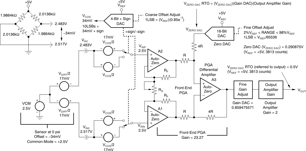
The resolution in either the positive or negative range is VREF/1200. For a +5V reference, this translates to 4.2mV steps. Figure 2-4 depicts the PGA309 with the gain settings used for the example bridge sensor application detailed in Section 2.1, Gain Scaling.

The conversion of the bridge initial differential offset plus its common-mode to the differential plus common-mode voltage source model is shown in Figure 2-4 for an initial bridge sensor offset of −34mV (VINP – VINN). Conceptually, this divides into two 17mV offset voltages with polarities as shown. If the coarse offset adjust is set for +34mV offset (VINP – VINN), then the initial bridge offset is canceled exactly. Any residual initial bridge offset not canceled by the coarse offset adjust will be gained up by the Front-End PGA gain and needs to be accounted for when setting the fine offset adjust by using the Zero DAC.
The coarse offset adjust is set by Register 4 bits (4:0), with bit 4 determining the coarse offset polarity as negative for a ‘1’ and positive for a ‘0’. The internal architecture of the coarse offset adjust does yield duplicate digital codes for both −7(VREF)(0.85e−3) and +7(VREF)(0.85e–3). See Section 6.2.5, Register 4, for a complete mapping of the coarse offset adjust settings.
The fine offset adjust is set by the Zero DAC. The Zero DAC setting is gained by the Gain DAC and the Output Amplifier gain and is referred-to-output (RTO). The Zero DAC is a unipolar, 16-bit DAC, with its reference being the VREF setting of the PGA309. The range of the Zero DAC is ensured to be linear from 2%VREF to 98%VREF, for VREF = +5V (for VREF < +5V, the upper end of the Zero DAC range can extend to VREF). The Zero DAC analog range is 0.1V ≤ Zero DAC analog range ≤ (VSA − 0.1V). The Zero DAC programming range is 0V ≤ Zero DAC programming range ≤ VREF. The data format is 16-bit unsigned. Register 1 bits (15:0) are used for the Zero DAC setting.