SBOU024C august 2004 – july 2023 PGA309
- 1
- Read This First
-
1Introduction
- 1.1 PGA309 Functional Description
- 1.2 Sensor Error Adjustment Range
- 1.3 Gain Scaling
- 1.4 Offset Adjustment
- 1.5 Voltage Reference
- 1.6 Sensor Excitation and Linearization
- 1.7 ADC for Temperature Sensing
- 1.8 External EEPROM and Temperature Coefficients
- 1.9 Fault Monitor
- 1.10 Over-Scale and Under-Scale Limits
- 1.11 Power-Up and Normal Operation
- 1.12 Digital Interface
- 1.13 Pin Configuration
- 2Detailed Description
- 3Operating Modes
-
4Digital Interface
- 4.1 Description
- 4.2 Two-Wire Interface
- 4.3 One-Wire Interface
- 4.4 One-Wire Interface Timeout
- 4.5 One-Wire Interface Timing Considerations
- 4.6 Two-Wire Access to External EEPROM
- 4.7 One-Wire Interface Initiated Two-Wire EEPROM Transactions
- 4.8 PGA309 Stand-Alone Mode and Two-Wire Transactions
- 4.9 PGA309 Two-Wire Bus Master Operation and Bus Sharing Considerations
- 4.10 One-Wire Operation with PRG Connected to VOUT
- 4.11 Four-Wire Modules and One-Wire Interface (PRG)
- 5Application Background
-
6Register Descriptions
- 6.1 Internal Register Overview
- 6.2
Internal Register Map
- 6.2.1 Register 0: Temp ADC Output Register (Read Only, Address Pointer = 00000)
- 6.2.2 Register 1: Fine Offset Adjust (Zero DAC) Register (Read/Write, Address Pointer = 00001)
- 6.2.3 Register 2: Fine Gain Adjust (Gain DAC) Register (Read/Write, Address Pointer = 00010)
- 6.2.4 Register 3: Reference Control and Linearization Register (Read/Write, Address Pointer = 00011)
- 6.2.5 Register 4: PGA Coarse Offset Adjust and Gain Select/Output Amplifier Gain Select Register (Read/Write, Address Pointer = 00100)
- 6.2.6 Register 5: PGA Configuration and Over/Under-Scale Limit Register (Read/Write, Address Pointer = 00101)
- 6.2.7 Register 6: Temp ADC Control Register (Read/Write, Address Pointer = 00110)
- 6.2.8 Register 7: Output Enable Counter Control Register (Read/Write, Address Pointer = 00111)
- 6.2.9 Register 8: Alarm Status Register (Read Only, Address Pointer = 01000)
- A External EEPROM Example
- B Detailed Block Diagram
- C Glossary
- Revision History
C Glossary
-
ADC
Analog-to-digital converter
-
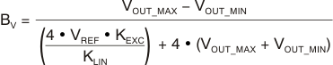
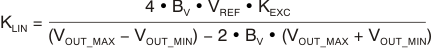
BV
Bridge nonlinearity with applied pressure.
-
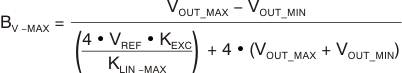
BV MAX
Maximum compensable nonlinearity
-
BV –MAX
-
BV +MAX

-
CF
External feedback capacitor connected between VSJ and VOUT, for stability.
-
CMR
Common-mode rejection
-
DAC
Digital-to-analog converter
-
EMI
Electromagnetic interference
-
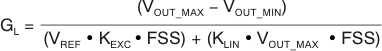
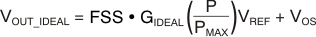
FSR
Full-scale range of PGA309 output.

-
FSS
Full-scale bridge sensitivity for sensor at PMAX (for example, 2mV/V).
-
GIDEAL
Ideal gain

-
GL
Gain of the PGA309 when using the Linearization circuit.
-
GNDA
Analog ground
-
GNDD
Digital ground
-
GT
Total gain produced by the PGA309 of VOUT/VIN gain.
GT = (Front-End PGA Gain)(Gain DAC)(Output Amplifier Gain)
-
IVR
Input voltage range of the PGA309.
-
KLIN
PGA linearization coefficient
-
KLIN –MAX
Most negative linearization coefficient. Its value is determined by the selected range of bridge sensor nonlinearity compensation.
-
KLIN +MAX
Most positive linearization coefficient. Its value is determined by the selected range of bridge sensor nonlinearity compensation.
-
KEXC
PGA excitation coefficient. Scale factor on VREF.
-
KP
Pressure constant. Converts linear input pressure to nonlinear pressure detected by sensor; referenced to full-scale input pressure.
-
LSB
Least significant bit
-
MSB
Most significant bit
-
P
Pressure input
-
PMIN
Minimum sensor input pressure
-
PMAX
Maximum sensor input pressure
-
PNL
Nonlinear pressure output of bridge with linear pressure input P.
-
POR
Power-on reset function
-
PRG
Single-wire interface program pin
-
RBRG
Bridge resistor value
-
RFB
External feedback resistor connected to VFB.
-
RFO
Internal feedback resistor for the Output Amplifier.
-
RFO EXT
Additional external feedback resistor for the Output Amplifier.
-
RGO
Internal gain resistor for the Output Amplifier.
-
RGO EXT
Additional external gain resistor for the Output Amplifier.
-
RISO
External isolation resistor connected to VOUT.
-
REFIN/REFOUT
Voltage reference input/output pin
-
RFI
Radio frequency interference
-
RTO
Referred-to-output
-
SCL
Clock input/output for Two-Wire serial interface
-
SDA
Data input/output for Two-Wire serial interface
-
TEMPIN
External temperature signal input
-
TEST
Test/external controller mode pin
-
VBRMAX
Maximum bridge sensor output
-
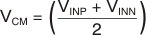
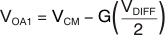
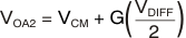
VCM
Common-mode voltage applied to the PGA309 input.
-
VCOS
Coarse offset voltage output of the coarse offset adjust DAC.
-
VDIFF
Differential voltage applied to the PGA309 inputs.
VDIFF = VINP − VINN
-
VEXC
Bridge sensor excitation voltage

-
VEXC MAX
Maximum bridge sensor excitation voltage

-
VEXC MIN
Minimum bridge sensor excitation voltage

-
VFB
VOUT feedback pin
-
VFRONT
The output of difference amplifier A3, of the Front-End PGA309.
-
VIN1
Signal input voltage 1
-
VIN2
Signal input voltage 2
-
VINN
The positive input of internal auto-zero amplifier A1, of the Front-End PGA.
-
VINP
The positive input of internal auto-zero amplifier A2, of the Front-End PGA.
-
VN
Output voltage of one branch of the bridge.
-
VOA1
Output voltage of internal auto-zero amplifier A1.
-
VOA2
Output voltage of internal auto-zero amplifier A2.
-
VOS
Sensor offset voltage
-
VOUT
Analog output voltage of conditioned sensor
-
VOUT ERR FSR
Error in %FSR of VOUT
-
VOUT FILT
Filtered VOUT
-
VOUT IDEAL
Ideal output for a given pressure, P.
-
VOUT MAX
VOUT for maximum bridge sensor output
-
VOUT MIN
VOUT for minimum bridge sensor output
-
VP
Output voltage of one branch of the bridge.
-
VREF
Reference voltage used by the PGA309 (internal or external).
-
VREFT
Temperature VREF
-
VS
Supply voltage
-
VSA
Analog supply voltage
-
VSD
Digital supply voltage
-
VSJ
Output Amplifier summing junction
-
VTEST
Test signal
-
VZERO DAC
Output voltage of the Zero DAC