SBOU024C august 2004 – july 2023 PGA309
- 1
- Read This First
-
1Introduction
- 1.1 PGA309 Functional Description
- 1.2 Sensor Error Adjustment Range
- 1.3 Gain Scaling
- 1.4 Offset Adjustment
- 1.5 Voltage Reference
- 1.6 Sensor Excitation and Linearization
- 1.7 ADC for Temperature Sensing
- 1.8 External EEPROM and Temperature Coefficients
- 1.9 Fault Monitor
- 1.10 Over-Scale and Under-Scale Limits
- 1.11 Power-Up and Normal Operation
- 1.12 Digital Interface
- 1.13 Pin Configuration
- 2Detailed Description
- 3Operating Modes
-
4Digital Interface
- 4.1 Description
- 4.2 Two-Wire Interface
- 4.3 One-Wire Interface
- 4.4 One-Wire Interface Timeout
- 4.5 One-Wire Interface Timing Considerations
- 4.6 Two-Wire Access to External EEPROM
- 4.7 One-Wire Interface Initiated Two-Wire EEPROM Transactions
- 4.8 PGA309 Stand-Alone Mode and Two-Wire Transactions
- 4.9 PGA309 Two-Wire Bus Master Operation and Bus Sharing Considerations
- 4.10 One-Wire Operation with PRG Connected to VOUT
- 4.11 Four-Wire Modules and One-Wire Interface (PRG)
- 5Application Background
-
6Register Descriptions
- 6.1 Internal Register Overview
- 6.2
Internal Register Map
- 6.2.1 Register 0: Temp ADC Output Register (Read Only, Address Pointer = 00000)
- 6.2.2 Register 1: Fine Offset Adjust (Zero DAC) Register (Read/Write, Address Pointer = 00001)
- 6.2.3 Register 2: Fine Gain Adjust (Gain DAC) Register (Read/Write, Address Pointer = 00010)
- 6.2.4 Register 3: Reference Control and Linearization Register (Read/Write, Address Pointer = 00011)
- 6.2.5 Register 4: PGA Coarse Offset Adjust and Gain Select/Output Amplifier Gain Select Register (Read/Write, Address Pointer = 00100)
- 6.2.6 Register 5: PGA Configuration and Over/Under-Scale Limit Register (Read/Write, Address Pointer = 00101)
- 6.2.7 Register 6: Temp ADC Control Register (Read/Write, Address Pointer = 00110)
- 6.2.8 Register 7: Output Enable Counter Control Register (Read/Write, Address Pointer = 00111)
- 6.2.9 Register 8: Alarm Status Register (Read Only, Address Pointer = 01000)
- A External EEPROM Example
- B Detailed Block Diagram
- C Glossary
- Revision History
2.1 Gain Scaling
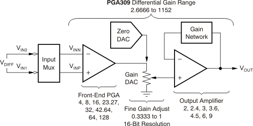
The PGA309 contains three main gain blocks for scaling differential input bridge sensor signals, as shown in Figure 2-1. The Front-End PGA contains the highest gain selection to allow for the highest signal-to-noise ratio by applying the largest gain at the front of the signal chain before the addition of other noise sources. The Front-End PGA gain select has eight gain settings (4, 8, 16, 23.27, 32, 42.67, 64, and 128) and is set by Register 4 bits (11:8). Bit 11 selects the polarity of the input mux.

The Front-End PGA is followed by the Gain DAC. The fine gain adjust is controlled by the 16-bit Gain DAC and is adjustable from 0.3333 to 1. Register 2 is used only for the Gain DAC setting.
Final signal gain is applied through the Output Amplifier, which has an internal select of seven gain settings (2, 2.4, 3, 3.6, 4.5, 6, 9). The Output Amplifier has a selection to disable the internal gain and allow user-supplied external resistors to set the Output Amplifier gain. Register 4 bits (14:12) select the internal Output Amplifier gains, except when programmed with ‘111’ when the internal feedback is disabled. The combined gain blocks allow for a VOUT/VDIFF signal gain of 2.666 (400kHz bandwidth) to 1152 (60kHz bandwidth).
The Front-End PGA of the PGA309 is a three op amp instrumentation amplifier for optimum rejection of common-mode voltages. This instrumentation amplifier is constructed using op amps with auto-zero front-ends to virtually eliminate 1/f noise.
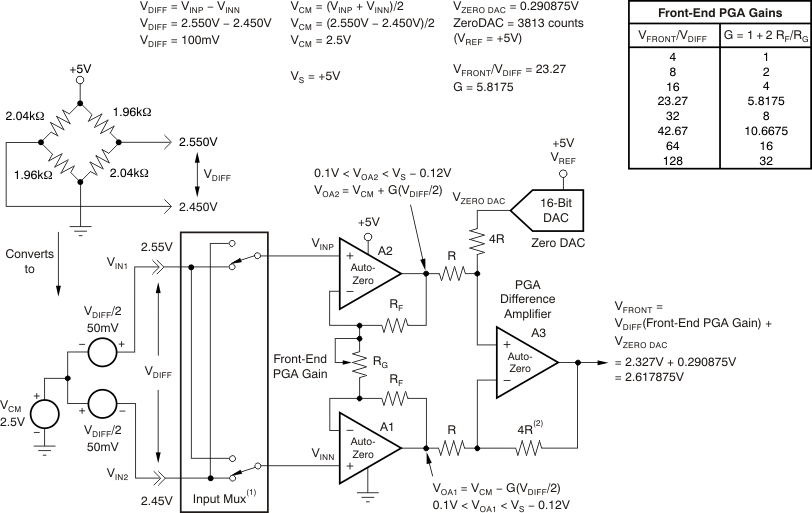
As with any instrumentation amplifier, there are limitations on the output voltage swing and input common-mode voltage range. The circuit in Figure 2-2 is representative of the Front-End PGA inside of the PGA309 and is used to evaluate critical internal node voltages to ensure that output voltage swing and common-mode limits are not violated. It is possible to violate the limits of these internal nodes and still have apparently valid output voltages at VOUT of the PGA309. There are internal comparators that can be set to monitor these internal nodes to indicate an out-of-limit condition during sensor calibration (see Section 2.8, Fault Monitor).

After choosing appropriate scaling for the PGA309 gain blocks, a simple hand analysis can check for internal node limit violations. It is important to convert the PGA309 input voltages (VINP, VINN) to common-mode and differential components for the maximum sensor output. The model for this conversion is illustrated in Figure 2-2. The Front-End PGA has a gain of 4 in difference amplifier A3. To analyze important internal nodes VOA1 and VOA2, it is necessary to assign the proper gain factor (G) to op amps A1 and A2. This is detailed in Figure 2-2 with the respective equations for the output voltages shown at the appropriate nodes. For maximum VDIFF output of the sensor, VOA1 and VOA2 are within the allowed voltage swing of: 0.1V < (VOA1 or VOA2) < VS − 0.12. Or, for this example: 0.1V < (VOA1 or VOA2) < 4.88V.
Other applications may yield different results that require different gain scaling or a resistor in the positive or negative leg of the sensor excitation path to adjust the common-mode input voltage of the PGA309. The maximum allowable input voltage range (IVR) of the PGA309 is specified as 0.2V < IVR < VSA − 1.5V, which for this application translates to 0.2V < IVR < 3.5V. In Figure 2-2 we see VINP = 2.550V and VINN = 2.450V, which is within the acceptable IVR specification.
The output (VFRONT) of difference amplifier A3 has a gain of 4 in it for voltages out of A2 and A1, but a gain of 1 for voltages out of the Zero DAC. VFRONT is shown with the contribution from VDIFF times the Front-End PGA gain plus the Zero DAC output voltage. The VFRONT signal is further processed through the Gain DAC and Output Amplifier gain blocks.
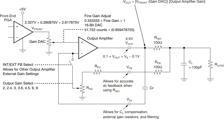
Figure 2-3 depicts the Gain DAC and Output Amplifier gain blocks inside the PGA309. For this example the Gain DAC was set to 0.859475571 and the Output Amplifer to a gain of 2. As shown in Figure 2-3, the net output voltage, VOUT, is 4.5V for the maximum VDIFF output of the sensor.
For VOUT MIN, the sensor output of 0V:
VOUT MIN = VZERO DAC [(Gain DAC)(Output Amplifier Gain)]
For this example:
VOUT MIN = 0.290908813V [(0.859475571)(2)] = 0.5000V
The Output Amplifier has external connections, which allow the end-user maximum flexibility in Output Amplifier configurations for a variety of applications. The use of the VFB and VSJ pins, are described in Section 2.4, Output Amplifier.
Example2-1 shows the procedure for solving for gain settings.
