SBOU124B march   2012  – july 2023 INA230


  1.   1
  2.   INA230EVM Evaluation Board and Software Tutorial
  3.   Trademarks
  4. 1Overview
    1. 1.1 INA230EVM Kit Contents
    2. 1.2 Related Documentation from Texas Instruments
  5. 2INA230EVM Hardware
    1. 2.1 Theory of Operation for INA230 Hardware
    2. 2.2 Signal Definitions of H1 (10-Pin Connector Socket)
      1. 2.2.1 Theory of Operation for SM-USB-DIG Platform
  6. 3INA230EVM (Rev A) Hardware Setup
    1. 3.1 Electrostatic Discharge Warning
    2. 3.2 Connecting the Hardware
    3. 3.3 Connecting Power
    4. 3.4 Connecting the USB Cable to the SM-USB-DIG Platform
    5. 3.5 INA230EVM Default Jumper Settings
    6. 3.6 INA230EVM Features
      1. 3.6.1 J2: I2C VS Control Setting
      2. 3.6.2 J3 and J4: I2C Address Hardware Setting (A0)
      3. 3.6.3 J5 and J6: I2C Address Hardware Setting (A1)
      4. 3.6.4 External I2C Lines and Terminal Block T1
      5. 3.6.5 VIN+ and VIN– Input Filter (R1, R2, and C1)
      6. 3.6.6 Shunt Monitor Configuration and Terminal Blocks T3 and T4
  7. 4INA230EVM Software Setup
    1. 4.1 Operating Systems for the INA230EVM Software
    2. 4.2 Software Installation
  8. 5INA230EVM Software Overview
    1. 5.1 Starting the INA230EVM Software
    2. 5.2 Configuring the INA230EVM Software
      1. 5.2.1 I2C Address Selection
      2. 5.2.2 Configure Operating Mode
      3. 5.2.3 Set Conversion Times
      4. 5.2.4 Set Configuration Register
      5. 5.2.5 Configuring the Alert Pin
    3. 5.3 Using the INA230EVM Software
      1. 5.3.1 INA230 Bus Voltage, Shunt Voltage, Current, and Power Reading Bar
      2. 5.3.2 Calculation and Theory of Operation
      3. 5.3.3 Register Tab
      4. 5.3.4 Graph Tab
      5. 5.3.5 Auto-Write and the Supply Voltage
  9. 6INA230EVM Documentation
    1. 6.1 Schematic
    2. 6.2 PCB Layout
    3. 6.3 Bill of Materials
  10. 7Revision History

Theory of Operation for INA230 Hardware

Figure 2-2 shows a block diagram of the INA230 test board hardware setup. The PCB provides connections to the I2C interface and general-purpose inputs and outputs (GPIOs) on the SM-USB-DIG Platform board. The PCB also provides connection points for external connections of the shunt voltage, bus voltage, and ground.
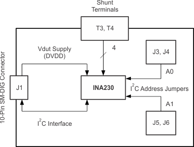
GUID-3EE2D67B-1651-42C2-AFD3-A56A4247884C-low.gifFigure 2-2 INA230EVM Test Board Block Diagram