SBOU180B november 2016 – july 2023 INA260
2.2 INA260EVM PCB Description
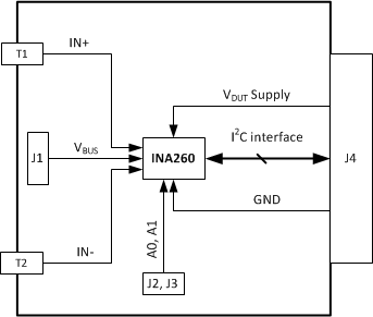
Figure 2-3 depicts a block diagram of the INA260EVM PCB highlighting the power supplies, analog inputs, and digital I/O signals.
 Figure 2-3 INA260EVM Block Diagram
The EVM PCB requires minimal instrumentation to be operated. In fact, the only pieces of required equipment not included in the kit are a ( Windows® 7) computer and an input current source. All other inputs are supplied by the SM-USB-DIG board, via the 10-pin connector socket, J4. Table 2-1 lists the pinout for J4.
Table 2-1 Signal Definition of J4 on
INA260EVM Board
| PIN ON J4 |
SIGNAL |
DESCRIPTION |
|---|---|---|
| 10 | I2C_SCL | I2C clock signal (SCL) |
| 9 | CTRL/MEAS4 | GPIO: control output or measure input |
| 8 | I2C_SDA1 | I2C data signal (SDA) |
| 7 | CTRL/MEAS5 | GPIO: control output or measure input |
| 6 | SPI_DOUT1 | SPI data output (MOSI) |
| 5 | VDUT | Switchable DUT power supply: 3.3 V, 5 V, Hi-Z (disconnected)(1) |
| 4 | SPI_CLK | SPI clock signal (SCLK) |
| 3 | GND | Power return (GND) |
| 2 | SPI_CS1 | SPI chip-select signal ( CS) |
| 1 | SPI_DIN1 | SPI data input (MISO) |
(1) When VDUT is Hi-Z, all digital I/Os are Hi-Z as well.