SBOU231 October 2020 OPA3S328
4 Power-Supply Connections
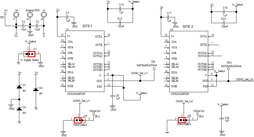
The power-supply connections for the OPA3S328EVM are provided through standard banana jack connectors J1, J2, and J3 at the top of the EVM. The OPA3S328EVM can be set up with a single unipolar supply or with dual bipolar supplies by setting jumper J11. Table 4-1 summarizes the pin definition for supply connector J1, J2, and J3 and the allowed voltage range for each supply connection when configured with either unipolar or bipolar supplies.
| Pin Number | Supply Connection | Voltage Range |
|---|---|---|
| J1 | (V+) supply |
Unipolar: 2.2 V to 5.5 V Bipolar: 1.1 V to 2.75 V |
| J2 | Analog Ground | 0 V |
|
J3 |
(V-) Supply |
Unipolar: Do not Connect Bipolar: –1.1 V to –2.75 V |
The EVM is configured by default to use a single unipolar supply by shunting jumper J11 pin 2–3. To configure the device with dual bipolar supply, set jumper J11 to shunt pin 1–2.
The digital ground pin (GND) of each site can be connected to analog ground or can be biased externally. The digital ground pin of site 1 is configured by setting jumper J16. Site 2 is configured by setting jumper J35. The EVM configures by default the digital ground connections to analog Ground by shunting pins 1–2. Place J16 and J35 to shunt pins 2–3 to bias the device digital GND to an external voltage through test points TP12 and TP34, respectively.
Figure 4-1 shows the J1, J2, and J3 standard banana supply connectors, and the jumpers J11, J34, and J35 configuration.
 Figure 4-1 OPA3S328EVM Voltage Supply Connections