SBOU263 April 2021 OPA3S2859
2.7 Layout Prints
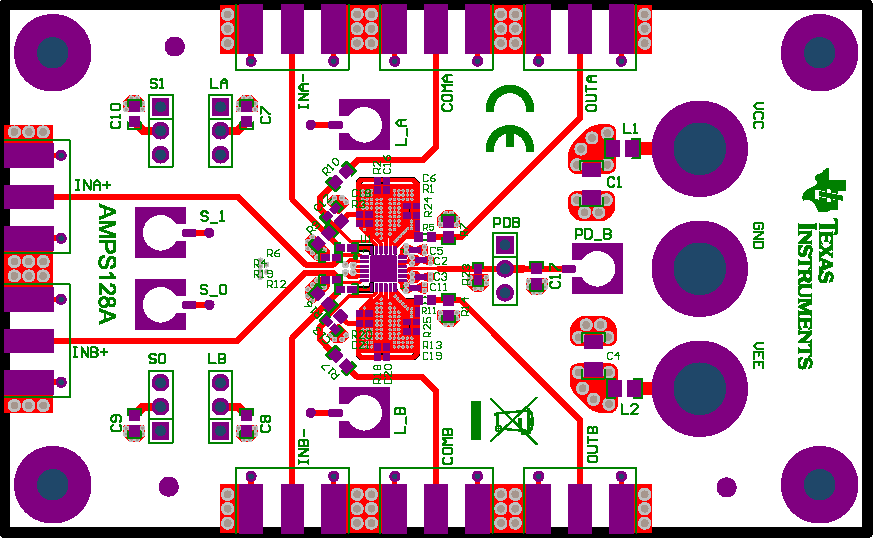 Figure 2-2 Top Layers
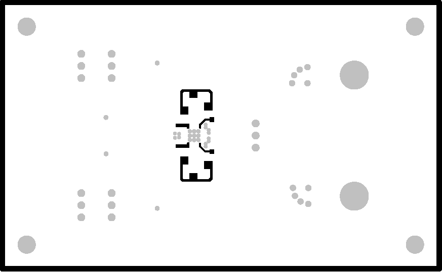 Figure 2-3 Ground Layer
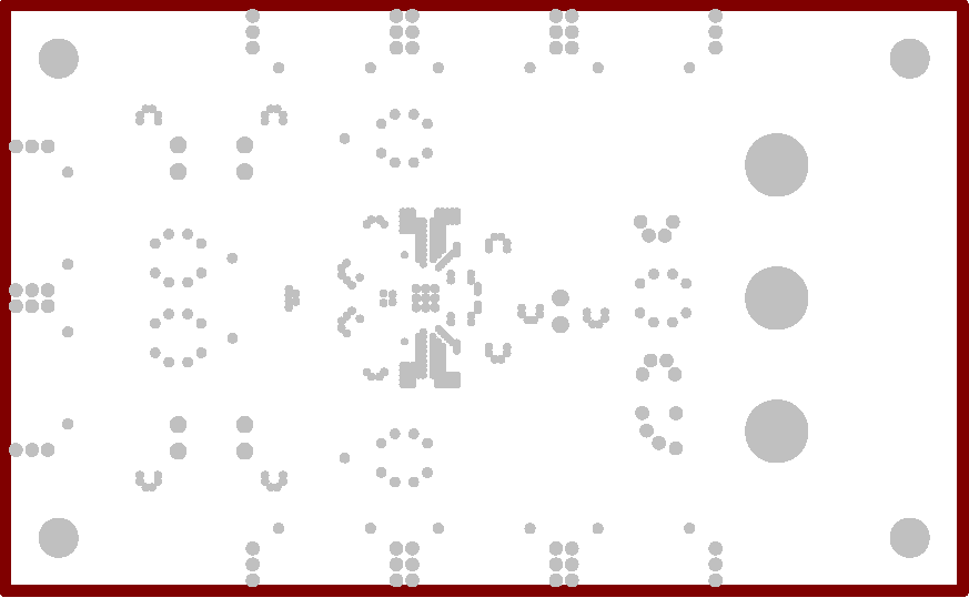 Figure 2-4 VCC Power Layer
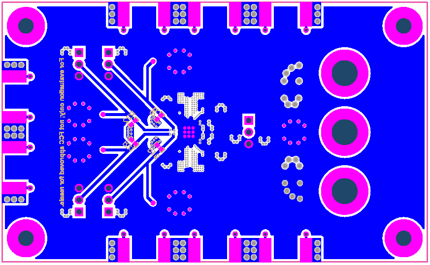 Figure 2-5 Bottom VEE and Signal Layers
SBOU263 April 2021 OPA3S2859
 Figure 2-2 Top Layers
 Figure 2-3 Ground Layer
 Figure 2-4 VCC Power Layer
 Figure 2-5 Bottom VEE and Signal Layers