SBOU272 November   2021 INA2126 , INA2128


  1.   Trademarks
  2. 1Overview
    1. 1.1 Features
    2. 1.2 INA Pinout
    3. 1.3 Compatible Devices
  3. 2Quick Start
    1. 2.1 Dual-Supply Configuration
    2. 2.2 Single-Supply Configuration
      1. 2.2.1 Direct Reference Connection
      2. 2.2.2 Buffered-Reference Voltage Connection
  4. 3EVM Components
    1. 3.1 Power
    2. 3.2 Inputs
      1. 3.2.1 Input Filtering
    3. 3.3 Output
      1. 3.3.1 Output Filtering
    4. 3.4 Reference
    5. 3.5 Miscellaneous
  5. 4Schematic, PCB Layout, and Bill of Materials
    1. 4.1 Schematic
    2. 4.2 PCB Layout
    3. 4.3 Bill of Materials

PCB Layout

The component PCB layout for the INA-DUAL-2AMP-EVM is shown in Figure 4-2.

Note: Figure 4-2 is intended to show how the board is laid out; it is not intended to be used for manufacturing PCBs.
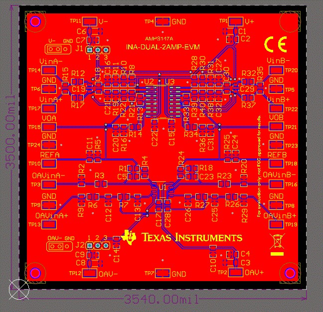
GUID-20210804-CA0I-JNCW-VXKN-JVWZRLPJQJJQ-low.jpg Figure 4-2 INA-DUAL-2AMP-EVM PCB