SBOU275 April   2022 INA190-EP


  1.   Trademarks
  2. 1Overview
    1. 1.1 INA190-EP Kit Contents
    2. 1.2 Related Documentation From Texas Instruments
  3. 2INA190EPEVM Hardware
    1. 2.1 Features
  4. 3Quick Start Setup and Use
    1. 3.1 Measurements
  5. 4INA190EPEVM Circuit and Components
    1. 4.1 R2x, R3x, R5x, C2x, C3x
    2. 4.2 C1x
    3. 4.3 R1x
    4. 4.4 R6
    5. 4.5 R4x
    6. 4.6 U1x - INA190-EP
    7. 4.7 J0x, J1x
  6. 5Reference Voltage Setup
    1. 5.1 Unidirectional Mode
    2. 5.2 Bidirectional Mode
  7. 6Guarding Voltage - Using the "Guarded Inputs" Panel
  8. 7INA190EPEVM Schematics and PCB Layout
    1. 7.1 Schematics
    2. 7.2 PCB Layout
  9. 8Bill of Materials

Schematics

Figure 7-1 through Figure 7-3 show the schematics for the INA190EPEVM PCB.

GUID-20220223-SS0I-TV5F-TLH6-N72SMBX7SSB2-low.gifFigure 7-1 INA190EPEVM Schematic - Gain A1 and Guarding Panels
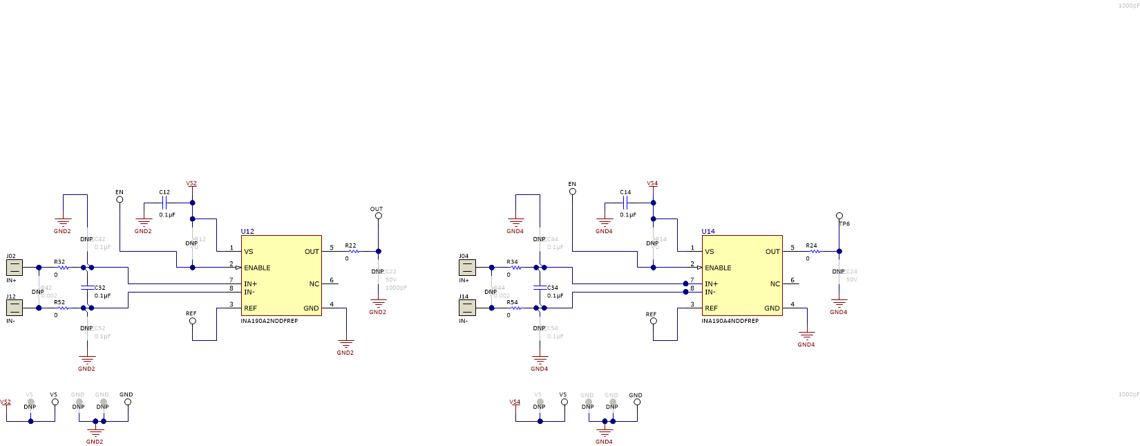
GUID-20220223-SS0I-RWDV-DNLH-BFGGHRSFFVLW-low.gifFigure 7-2 INA190EPEVM Schematic - Gain A2 and A4 Panels
GUID-20220223-SS0I-71Z4-HNRD-KGNBBJPDHMZR-low.gifFigure 7-3 INA190EPEVM Schematic - Gain A3 and A5 Panels