SBOU293E November   2022  – August 2024


  1.   1
  2.   Description
  3.   Features
  4.   4
  5. 1Evaluation Module Overview
    1. 1.1 Introduction
    2. 1.2 OPTEVM Kit Contents
    3. 1.3 Device Information
  6. 2Hardware
    1. 2.1 OPTEVM Hardware Overview
  7. 3Software
    1. 3.1 OPTEVM Software
      1. 3.1.1 Hardware Requirements
      2. 3.1.2 Software Installation
      3. 3.1.3 Typical OPTEVM Hardware Setup
      4. 3.1.4 Launching the OPT300x/4xxxEVM Software
      5. 3.1.5 OPTEVM Software Operation
        1. 3.1.5.1 Getting Started
        2. 3.1.5.2 Feature Descriptions
          1. 3.1.5.2.1 Lux Plot
          2. 3.1.5.2.2 Mean, Std, and the Blue Slider
      6. 3.1.6 Controls
        1. 3.1.6.1 Capture Controls
          1. 3.1.6.1.1 Start Capture and Stop Capture
          2. 3.1.6.1.2 Display Sample Count
          3. 3.1.6.1.3 Save to File
        2. 3.1.6.2 Device Controls
          1. 3.1.6.2.1 Mode Select
          2. 3.1.6.2.2 Conversion Time
        3. 3.1.6.3 Operation Controls
          1. 3.1.6.3.1 Operation Select
          2. 3.1.6.3.2 Measurement/Capture Trigger
          3. 3.1.6.3.3 Oneshot Time (μs)
      7. 3.1.7 OPTxxxDTSEVM Variants
        1. 3.1.7.1 OPT4048DTSEVM
          1. 3.1.7.1.1 OPT4048DTSEVM CIE XY Window
          2. 3.1.7.1.2 OPT4048DTSEVM Lux Live Window
          3. 3.1.7.1.3 OPT4048DTSEVM Channel Live Window
        2. 3.1.7.2 OPT4060DTSEVM
          1. 3.1.7.2.1 OPT4060DTSEVM Channel Live Window
          2. 3.1.7.2.2 OPT4060DTSEVM Lux Live Window
      8. 3.1.8 Scripts Window
        1. 3.1.8.1 Additional Features of the Scripts Window
          1. 3.1.8.1.1 Hidden IDE Window
          2. 3.1.8.1.2 devInit.py
          3. 3.1.8.1.3 04-launchGUI.py
        2. 3.1.8.2 Overview of Device Registers: OPT4xxx Devices
  8. 4Hardware Design Files
    1. 4.1 Coupon Board
      1. 4.1.1 Schematic
      2. 4.1.2 PCB Layout DTS Package
      3. 4.1.3 Bill of Materials (BOM)
    2. 4.2 Motherboard
      1. 4.2.1 Schematic
      2. 4.2.2 PCB Layout
      3. 4.2.3 Bill of Materials
  9. 5Additional Information
    1. 5.1 Trademarks
    2. 5.2 Troubleshooting
      1. 5.2.1 Microsoft Windows 7 Manual Driver Installation
  10. 6Related Documentation from Texas Instruments
  11. 7Revision History

PCB Layout

Figure 5-2 and Figure 5-3 show the top and bottom PCB layers, respectively, of the test board. Figure 5-4 and Figure 5-5 show the assembly drawings of the top and bottom PCB layers, respectively.
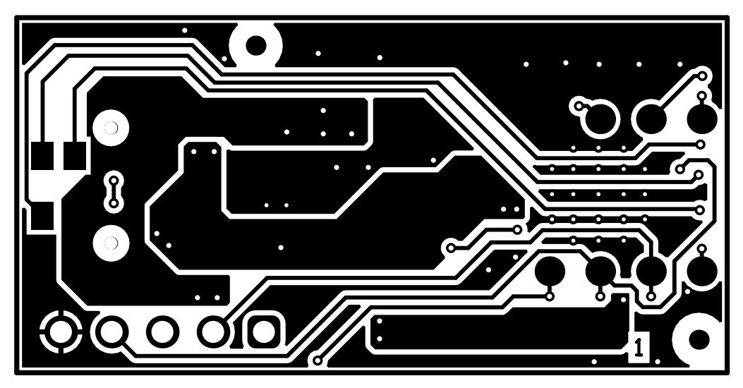
OPT3005DTSEVM OPT3005EVM OPT4001DTSEVM OPT4048DTSEVM PCB Top
                    LayerFigure 4-7 PCB Top Layer
OPT3005DTSEVM OPT3005EVM OPT4001DTSEVM OPT4048DTSEVM PCB
                    Bottom LayerFigure 4-8 PCB Bottom Layer
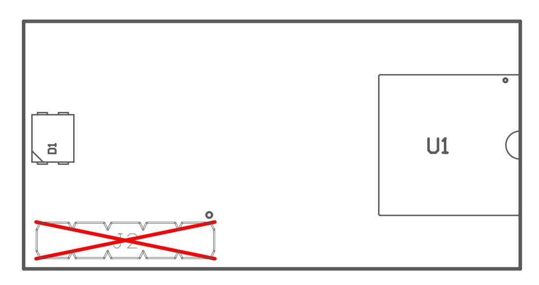
OPT3005DTSEVM OPT3005EVM OPT4001DTSEVM OPT4048DTSEVM PCB Top-Layer Assembly
                    DrawingFigure 4-9 PCB Top-Layer Assembly Drawing
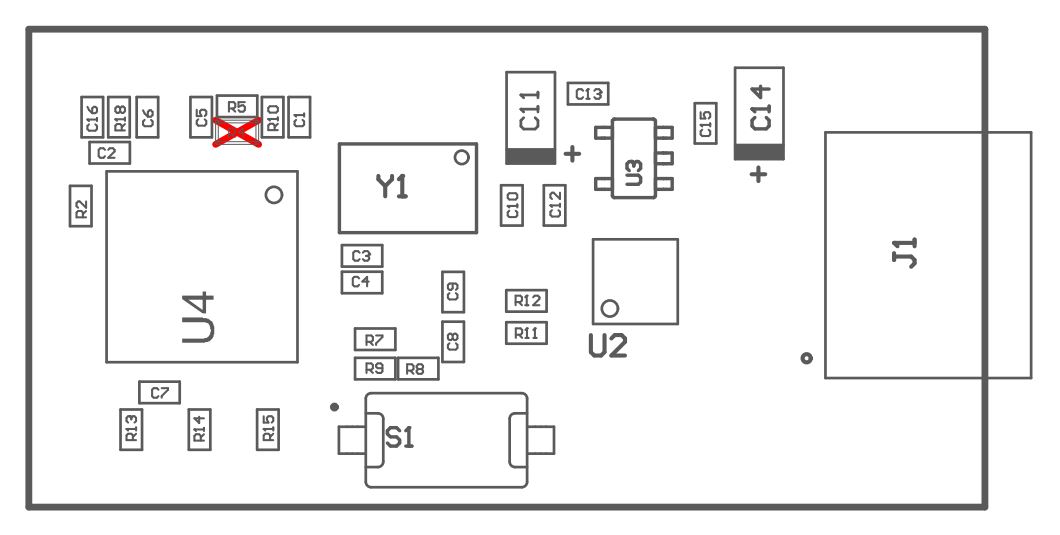
OPT3005DTSEVM OPT3005EVM OPT4001DTSEVM OPT4048DTSEVM PCB Bottom-Layer Assembly
                    DrawingFigure 4-10 PCB Bottom-Layer Assembly Drawing