SBVA086A June 2020 – November 2024 TPS7B84-Q1
4.1 VSON Package
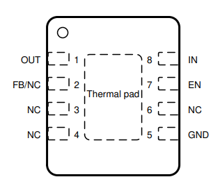
Figure 4-1 shows the TPS7B84-Q1 pin diagram for the VSON package. For a detailed description of the device pins refer to the Pin Configuration and Functions section in the TPS7B84-Q1 data sheet.
 Figure 4-1 Pin Diagram (VSON Package)
Table 4-2 Pin FMA for Device Pins
Short-Circuited to Ground
| Pin Name | Pin No. | Description of Potential Failure Effects | Failure Effect Class |
|---|---|---|---|
| OUT | 1 | Regulation is not possible, the device operates at current limit. The device can cycle in and out of thermal shutdown. | B |
| NC, FB | 2 | (Fixed) No effect. Normal operation. | D |
| (Adjustable) The device operates as a switch in dropout mode. The output tracks VIN - VDO. | B | ||
| NC | 3, 4, 6 | No effect. Normal operation. | D |
| GND | 5 | No effect. Normal operation. | D |
| EN | 7 | The device is disabled, resulting in no output voltage. | B |
| IN | 8 | Power is not supplied to the device. | B |
Table 4-3 Pin FMA for Device Pins
Open-Circuited
| Pin Name | Pin No. | Description of Potential Failure Effects | Failure Effect Class |
|---|---|---|---|
| OUT | 1 | The device output is disconnected from the load. | B |
| NC, FB | 2 | (Fixed) No effect. Normal operation. | D |
| (Adjustable) The device state is unknown. If the device is on, the output voltage is indeterminate. | B | ||
| NC | 3, 4, 6 | No effect. Normal operation. | D |
| GND | 5 | There is no current loop for the supply voltage. The device does not regulate and is at risk of exceeding absolute maximum conditions. | A |
| EN | 7 | Device not turning on is possible. | B |
| IN | 8 | Power is not supplied to the device. | B |
Table 4-4 Pin FMA for Device Pins
Short-Circuited to Adjacent Pin
| Pin Name | Pin No. | Shorted to (1) | Description of Potential Failure Effects | Failure Effect Class |
|---|---|---|---|---|
| OUT | 1 | NC, FB | (Fixed) No effect. Normal operation. | D |
| (Adjustable) Normal operation if using the device in unity gain. | D | |||
| (Adjustable) If not using the device in unity gain, connecting OUT to FB results in a low output voltage. | B | |||
| NC, FB | 2 | NC | No effect. Normal operation. | D |
| NC | 3 | NC | No effect. Normal operation. | D |
| GND | 5 | NC | No effect. Normal operation | D |
| NC | 6 | EN | No effect. Normal operation. | D |
| EN | 7 | IN | The device remains on. Regulation is possible. | C |
(1) In the event of a 10kΩ short
between adjacent pins, there is no change in the potential failure effect or
class.
Table 4-5 Pin FMA for Device Pins
Short-Circuited to Supply
| Pin Name | Pin No. | Description of Potential Failure Effects | Failure Effect Class |
|---|---|---|---|
| OUT | 1 | Regulation is not possible. VOUT = VIN. If VIN exceeds 20V, damage is possible. | A |
| NC, FB | 2 | (Fixed) No effect. Normal operation. | D |
| (Adjustable) The device having no output voltage is possible. | B | ||
| NC | 3, 4, 6 | No effect. Normal operation. | D |
| GND | 5 | Power is not supplied to the device. | B |
| EN | 7 | The device remains on. Regulation is possible. | C |
| IN | 8 | No effect. Normal operation. | D |