SBVA092 June 2022 TPS7A14
1.2 Biasing Rail for NMOS LDO
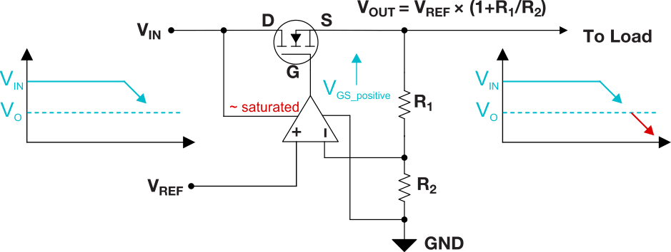
LDO, especially pass element(dealing MOSFET only here) works in the linear region to reduce the input voltage down to the required output voltage and it is controlled by error amplifier changing FET’s gate to the appropriate operating point at a given load condition, or accordingly when the input voltage changes. Key note is that the pass element behaves like a simple resistor. We understand drain-to-source resistance Rds is moving its value inside linear region area of MOSFET. If we consider only pass element, conventional background says that N-type power stage has higher dropout limitation than that of P-type and it’s true that because error amplifier will saturate at the input supply voltage as Vin approached to Vout. Figure 1-2 illustrates the mechanism.
 Figure 1-2 Dropout Limitation of NMOS LDO
 As Vin approaches Vout, error amplifier compensates it through lowering the Rds in order to maintain regulation. However, since the collapsing Vin supplies the amplifier VGS cannot be more positively increased at a certain point. It results in unregulated Vout. Limited Rds multiplied by output load current will derive more dropout from nominal Vout. That’s because there are two options to overcome this challenge. One is to have external biasing for gate driving and the other one is a charge pump.
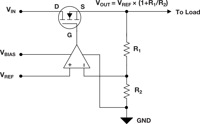
 Figure 1-3 NMOS LDO with an External Biasing
VBIAS serves as the positive supply rail for error amplifier and allows its output to swing up to VBIAS. Now though Vin approaches Vout, driver circuit enables maintaining a high VGS. This makes Rds lower achieving ultra low dropout performance. Note that minimum bias voltage above the nominal desired Vout must be maintained. The information about minimum VBIAS headroom is provided commonly in the product data sheet.