SBVS037Q August   2003  – September 2024 TPS732

PRODUCTION DATA  

  1.   1
  2. Features
  3. Applications
  4. Description
  5. Pin Configuration and Functions
  6. Specifications
    1. 5.1 Absolute Maximum Ratings
    2. 5.2 ESD Ratings
    3. 5.3 Recommended Operating Conditions
    4. 5.4 Thermal Information
    5. 5.5 Thermal Information
    6. 5.6 Electrical Characteristics
    7. 5.7 Switching Characteristics
    8. 5.8 Typical Characteristics
  7. Detailed Description
    1. 6.1 Overview
    2. 6.2 Functional Block Diagrams
    3. 6.3 Feature Description
      1. 6.3.1 Output Noise
      2. 6.3.2 Internal Current Limit
      3. 6.3.3 Enable Pin and Shutdown
      4. 6.3.4 Dropout Voltage
      5. 6.3.5 Reverse Current
    4. 6.4 Device Functional Modes
      1. 6.4.1 Normal Operation With 1.7V ≤ VIN ≤ 5.5V and VEN ≥ 1.7V
  8. Application and Implementation
    1. 7.1 Application Information
    2. 7.2 Typical Application
      1. 7.2.1 Design Requirements
      2. 7.2.2 Detailed Design Procedure
        1. 7.2.2.1 Input and Output Capacitor Requirements
        2. 7.2.2.2 Transient Response
      3. 7.2.3 Application Curves
    3. 7.3 Power Supply Recommendations
    4. 7.4 Layout
      1. 7.4.1 Layout Guidelines
        1. 7.4.1.1 Thermal Considerations
          1. 7.4.1.1.1 Power Dissipation
      2. 7.4.2 Layout Examples
  9. Device and Documentation Support
    1. 8.1 Device Support
      1. 8.1.1 Development Support
        1. 8.1.1.1 Evaluation Modules
        2. 8.1.1.2 Spice Models
      2. 8.1.2 Device Nomenclature
    2. 8.2 Documentation Support
      1. 8.2.1 Related Documentation
    3. 8.3 Receiving Notification of Documentation Updates
    4. 8.4 Support Resources
    5. 8.5 Trademarks
    6. 8.6 Electrostatic Discharge Caution
    7. 8.7 Glossary
  10. Revision History
  11. 10Mechanical, Packaging, and Orderable Information

Transient Response

The low open-loop output impedance provided by the NMOS pass transistor in a voltage follower configuration allows operation without an output capacitor for many applications. As with any regulator, the addition of a capacitor (nominal value 1μF) from the OUT pin to ground reduces undershoot magnitude but increases the duration. In the adjustable version, the addition of a capacitor, CFB, from the OUT pin to the FB pin also improves transient response.

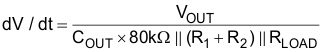
The TPS732 does not have active pulldown when the output is overvoltage. This feature allows applications that connect higher voltage sources, such as alternate power supplies, to the output. This feature also results in an output overshoot of several percent if the load current quickly drops to zero when a capacitor is connected to the output. The duration of overshoot is reduced by adding a load resistor. The overshoot decays at a rate determined by output capacitor COUT and the internal or external load resistance. The rate of decay is given by:

(Fixed voltage versions)

Equation 4. TPS732

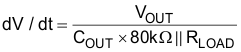
(Adjustable voltage version)

Equation 5. TPS732