SBVS037Q August 2003 – September 2024 TPS732
PRODUCTION DATA
- 1
- 1 Features
- 2 Applications
- 3 Description
- 4 Pin Configuration and Functions
- 5 Specifications
- 6 Detailed Description
- 7 Application and Implementation
- 8 Device and Documentation Support
- 9 Revision History
- 10Mechanical, Packaging, and Orderable Information
6.3.1 Output Noise
A precision band-gap reference is used to generate the internal reference voltage, VREF. This reference is the dominant noise source within the TPS732 and generates approximately 32µVRMS (10Hz to 100kHz) at the reference output (NR). The regulator control loop gains up the reference noise with the same gain as the reference voltage, so that the noise voltage of the regulator is approximately given by:
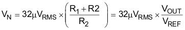
Because the value of VREF is 1.2V, this relationship reduces to:
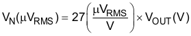
An internal 27kΩ resistor in series with the noise-reduction pin (NR) forms a low-pass filter for the voltage reference when an external noise-reduction capacitor, CNR, is connected from NR to ground. For CNR = 10nF, the total noise in the 10Hz to 100kHz bandwidth is reduced by a factor of approximately 3.2, giving the approximate relationship:
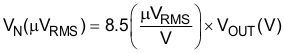
for CNR = 10nF.
This noise-reduction effect is shown as RMS Noise Voltage vs CNR (Figure 5-33) in the Typical Characteristics section.
The TPS73201 adjustable version does not have the NR pin available. However, connecting a feedback capacitor, CFB, from the output to the feedback pin (FB) reduces output noise and improves load transient performance.
The TPS732 uses an internal charge pump to develop an internal supply voltage sufficient to drive the gate of the NMOS pass transistor above VOUT. The charge pump generates approximately 250μV of switching noise at approximately 4MHz; however, charge-pump noise contribution is negligible at the output of the regulator for most values of IOUT and COUT.