SBVS067U January   2006  – September 2024 TPS737

PRODUCTION DATA  

  1.   1
  2. Features
  3. Applications
  4. Description
  5. Pin Configuration and Functions
  6. Specifications
    1. 5.1 Absolute Maximum Ratings
    2. 5.2 ESD Ratings
    3. 5.3 Recommended Operating Conditions
    4. 5.4 Thermal Information
    5. 5.5 Thermal Information
    6. 5.6 Electrical Characteristics
    7. 5.7 Typical Characteristics
  7. Detailed Description
    1. 6.1 Overview
    2. 6.2 Functional Block Diagrams
    3. 6.3 Feature Description
      1. 6.3.1 Output Noise
      2. 6.3.2 Internal Current Limit
      3. 6.3.3 Enable Pin and Shutdown
      4. 6.3.4 Reverse Current
    4. 6.4 Device Functional Modes
  8. Application and Implementation
    1. 7.1 Application Information
    2. 7.2 Typical Application
      1. 7.2.1 Design Requirements
      2. 7.2.2 Detailed Design Procedure
        1. 7.2.2.1 Input and Output Capacitor Requirements
        2. 7.2.2.2 Dropout Voltage
        3. 7.2.2.3 Transient Response
      3. 7.2.3 Application Curves
    3. 7.3 Best Design Practices
    4. 7.4 Power Supply Recommendations
    5. 7.5 Layout
      1. 7.5.1 Layout Guidelines
        1. 7.5.1.1 Power Dissipation
        2. 7.5.1.2 Thermal Protection
        3. 7.5.1.3 Estimating Junction Temperature
      2. 7.5.2 Layout Example
  9. Device and Documentation Support
    1. 8.1 Device Support
      1. 8.1.1 Development Support
        1. 8.1.1.1 Evaluation Modules
        2. 8.1.1.2 Spice Models
      2. 8.1.2 Device Nomenclature
    2. 8.2 Documentation Support
      1. 8.2.1 Related Documentation
    3. 8.3 Receiving Notification of Documentation Updates
    4. 8.4 Support Resources
    5. 8.5 Trademarks
    6. 8.6 Electrostatic Discharge Caution
    7. 8.7 Glossary
  10. Revision History
  11. 10Mechanical, Packaging, and Orderable Information

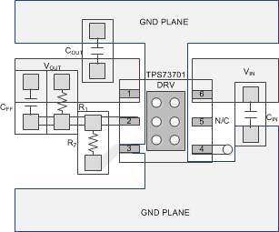
Layout Example

TPS737 Layout
                    Example Figure 7-12 Layout Example
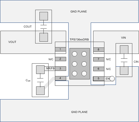
TPS737 Fixed
                    Output Voltage Option Layout (DRB Package) Figure 7-13 Fixed Output Voltage Option Layout (DRB Package)
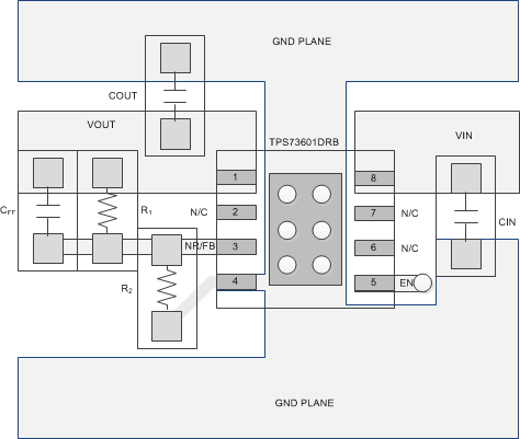
TPS737 Adjustable Output Voltage Option Layout (DRB Package) Figure 7-14 Adjustable Output Voltage Option Layout (DRB Package)
TPS737 Layout Example for the DCQ
                    Package Fixed Version Figure 7-15 Layout Example for the DCQ Package Fixed Version
TPS737 Layout Example for the DCQ
                    Package Adjustable Version Figure 7-16 Layout Example for the DCQ Package Adjustable Version