SBVS067U January   2006  – September 2024 TPS737

PRODUCTION DATA  

  1.   1
  2. Features
  3. Applications
  4. Description
  5. Pin Configuration and Functions
  6. Specifications
    1. 5.1 Absolute Maximum Ratings
    2. 5.2 ESD Ratings
    3. 5.3 Recommended Operating Conditions
    4. 5.4 Thermal Information
    5. 5.5 Thermal Information
    6. 5.6 Electrical Characteristics
    7. 5.7 Typical Characteristics
  7. Detailed Description
    1. 6.1 Overview
    2. 6.2 Functional Block Diagrams
    3. 6.3 Feature Description
      1. 6.3.1 Output Noise
      2. 6.3.2 Internal Current Limit
      3. 6.3.3 Enable Pin and Shutdown
      4. 6.3.4 Reverse Current
    4. 6.4 Device Functional Modes
  8. Application and Implementation
    1. 7.1 Application Information
    2. 7.2 Typical Application
      1. 7.2.1 Design Requirements
      2. 7.2.2 Detailed Design Procedure
        1. 7.2.2.1 Input and Output Capacitor Requirements
        2. 7.2.2.2 Dropout Voltage
        3. 7.2.2.3 Transient Response
      3. 7.2.3 Application Curves
    3. 7.3 Best Design Practices
    4. 7.4 Power Supply Recommendations
    5. 7.5 Layout
      1. 7.5.1 Layout Guidelines
        1. 7.5.1.1 Power Dissipation
        2. 7.5.1.2 Thermal Protection
        3. 7.5.1.3 Estimating Junction Temperature
      2. 7.5.2 Layout Example
  9. Device and Documentation Support
    1. 8.1 Device Support
      1. 8.1.1 Development Support
        1. 8.1.1.1 Evaluation Modules
        2. 8.1.1.2 Spice Models
      2. 8.1.2 Device Nomenclature
    2. 8.2 Documentation Support
      1. 8.2.1 Related Documentation
    3. 8.3 Receiving Notification of Documentation Updates
    4. 8.4 Support Resources
    5. 8.5 Trademarks
    6. 8.6 Electrostatic Discharge Caution
    7. 8.7 Glossary
  10. Revision History
  11. 10Mechanical, Packaging, and Orderable Information

Description

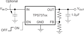
The TPS737 linear low-dropout (LDO) voltage regulator uses an NMOS pass transistor in a voltage-follower configuration. This topology is relatively insensitive to the output capacitor value and ESR, allowing for a wide variety of load configurations. Load transient response is excellent, even with a small 1μF ceramic output capacitor. The NMOS topology also allows for very low dropout.

The TPS737 uses an advanced BiCMOS process to yield high precision while delivering very low dropout voltages and low ground pin current. Devices that use the latest manufacturing flow have an updated design with new silicon on the latest TI process technology. Current consumption, when not enabled, is less than 20nA and is designed for portable applications. This device is protected by thermal shutdown and foldback current limit.

For applications that require higher output voltage accuracy, consider TI's TPS7A37 1% overall accuracy, 1A low-dropout voltage regulator.

Package Information
PART NUMBERPACKAGE(1)PACKAGE SIZE(2)
TPS737DRB (VSON, 8)3mm × 3mm
DCQ (SOT-223, 6)6.5mm × 7.06mm
DRV (WSON, 6)2mm × 2mm
For more information, see the Section 10.
The package size (length × width) is a nominal value and includes pins, where applicable.


TPS737 Typical Application CircuitTypical Application Circuit