SBVS074N January   2007  – June 2024 TPS74801

PRODUCTION DATA  

  1.   1
  2. Features
  3. Applications
  4. Description
  5. Pin Configuration and Functions
  6. Specifications
    1. 5.1 Absolute Maximum Ratings
    2. 5.2 ESD Ratings
    3. 5.3 Recommended Operating Conditions
    4. 5.4 Thermal Information
    5. 5.5 Electrical Characteristics
    6. 5.6 Typical Characteristics: IOUT = 50 mA
    7. 5.7 Typical Characteristics: IOUT = 1 A
  7. Detailed Description
    1. 6.1 Overview
    2. 6.2 Functional Block Diagrams
    3. 6.3 Feature Description
      1. 6.3.1 Enable/Shutdown
      2. 6.3.2 Power Good
      3. 6.3.3 Internal Current Limit
      4. 6.3.4 Thermal Protection
    4. 6.4 Device Functional Modes
      1. 6.4.1 Normal Operation
      2. 6.4.2 Dropout Operation
      3. 6.4.3 Disabled
    5. 6.5 Programming
      1. 6.5.1 Programmable Soft-Start
      2. 6.5.2 Sequencing Requirements
  8. Application and Implementation
    1. 7.1 Application Information
      1. 7.1.1 Adjusting the Output Voltage
      2. 7.1.2 Input, Output, and Bias Capacitor Requirements
      3. 7.1.3 Transient Response
      4. 7.1.4 Dropout Voltage
      5. 7.1.5 Output Noise
    2. 7.2 Typical Applications
      1. 7.2.1 FPGA I/O Supply at 1.5 V With a Bias Rail
        1. 7.2.1.1 Design Requirements
        2. 7.2.1.2 Detailed Design Procedure
        3. 7.2.1.3 Application Curves
      2. 7.2.2 FPGA I/O Supply at 1.5 V Without a Bias Rail
        1. 7.2.2.1 Design Requirements
        2. 7.2.2.2 Detailed Design Procedure
        3. 7.2.2.3 Application Curves
    3. 7.3 Power Supply Recommendations
    4. 7.4 Layout
      1. 7.4.1 Layout Guidelines
        1. 7.4.1.1 Estimating Junction Temperature
      2. 7.4.2 Layout Example
  9. Device and Documentation Support
    1. 8.1 Device Support
      1. 8.1.1 Device Nomenclature
      2. 8.1.2 Development Support
        1. 8.1.2.1 Evaluation Modules
        2. 8.1.2.2 Spice Models
    2. 8.2 Documentation Support
      1. 8.2.1 Related Documentation
    3. 8.3 Receiving Notification of Documentation Updates
    4. 8.4 Support Resources
    5. 8.5 Trademarks
    6. 8.6 Electrostatic Discharge Caution
    7. 8.7 Glossary
  10. Revision History
  11. 10Mechanical, Packaging, and Orderable Information

Description

The TPS748 low-dropout (LDO) linear regulator provides an easy-to-use robust power management solution for a wide variety of applications. User-programmable soft-start minimizes stress on the input power source by reducing capacitive inrush current on start-up. The soft-start is monotonic and designed for powering many different types of processors and ASICs. The enable input and power-good output allow easy sequencing with external regulators. This complete flexibility allows a solution to be configured that meets the sequencing requirements of FPGAs, DSPs, and other applications with special start-up requirements.

A precision reference and error amplifier deliver 1% accuracy (new chip) over load, line, temperature, and process. The device is stable with any type of capacitor greater than or equal to 2.2μF, and is fully specified for TJ = –40°C to +125°C. The TPS748 is offered in a small, 3mm × 3mm, VSON-10 package, yielding a highly compact, total solution size. The device is also available in a 5mm × 5mm VQFN-20 package for compatibility with the TPS742.

Package Information
PART NUMBER PACKAGE(1) PACKAGE SIZE(2)
TPS748 DRC (VSON, 10) 3mm × 3mm
RGW (VQFN, 20) 5mm × 5mm
For more information, see the Mechanical, Packaging, and Orderable Information.
The package size (length × width) is a nominal value and includes pins, where applicable.


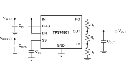
TPS748 Typical Application Circuit
                        (Adjustable)Typical Application Circuit (Adjustable)
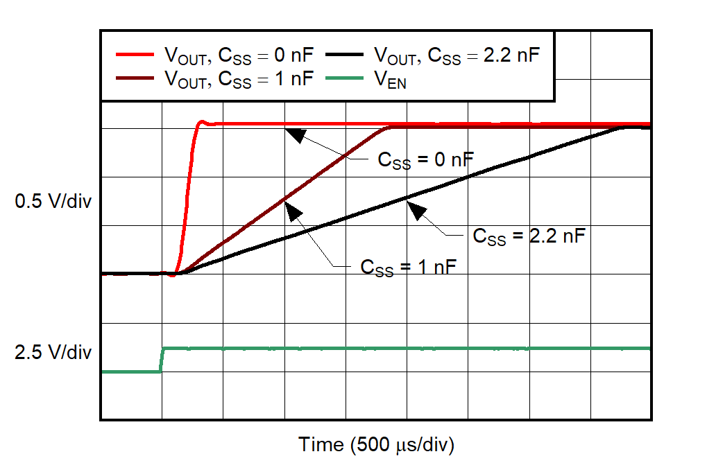
TPS748 Turn-On ResponseTurn-On Response