SBVS099H november 2007 – april 2023 TPS74701
PRODUCTION DATA
- 1 Features
- 2 Applications
- 3 Description
- 4 Revision History
- 5 Pin Configuration and Functions
-
6 Specifications
- 6.1 Absolute Maximum Ratings
- 6.2 ESD Ratings
- 6.3 Recommended Operating Conditions
- 6.4 Thermal Information
- 6.5 Electrical Characteristics: Other Orderable Devices (non-M3 Suffix)
- 6.6 Electrical Characteristics: Orderable Device (M3 Suffix)
- 6.7 Typical Characteristics: VEN = VIN (All Other Orderable Devices, Non-M3 Suffix)
- 6.8 Typical Characteristics: VEN = VIN = 1.8 V, VOUT = 1.5 V (All Other Orderable Devices, Non-M3 Suffix)
- 6.9 Typical Characteristics: IOUT = 50 mA (M3 Suffix)
- 6.10 Typical Characteristics: VEN = VIN = 1.8 V, VOUT = 1.5 V (M3 Suffix)
- 7 Detailed Description
- 8 Application and Implementation
- 9 Device and Documentation Support
- 10Mechanical, Packaging, and Orderable Information
3 Description
The TPS74701 low-dropout (LDO) linear regulator provides an easy-to-use, robust power management solution for a wide variety of applications. User-programmable soft-start minimizes stress on the input power source by reducing capacitive inrush current on start-up. The soft-start is monotonic and designed for powering many different types of processors and application-specific integrated circuits (ASICs). The enable input and power-good output allow easy sequencing with external regulators. This complete flexibility allows a solution to be configured that meets the sequencing requirements of field-programmable gate arrays (FPGAs), digital signal processors (DSPs), and other applications with special start-up requirements.
A precision reference and error
amplifier deliver 2% accuracy over load, line, temperature, and process. The device
is stable with any type of capacitor greater than or equal to 2.2 μF, and is fully
specified from
–40°C to +125°C. The TPS74701 is
offered in a small 3-mm × 3-mm VSON-10 package for compatibility with the TPS74801.
| PART NUMBER | PACKAGE(1) | BODY SIZE (NOM) |
|---|---|---|
| TPS74701 | DRC (VSON, 10) | 3.00 mm × 3.00 mm |
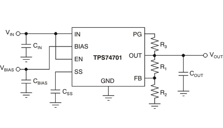
 Typical Application Circuit
(Adjustable)
 Turn-On Response