SBVS128F June   2009  – December 2015 TPS727

PRODUCTION DATA.  

  1. Features
  2. Applications
  3. Description
  4. Revision History
  5. Pin Configurations and Functions
  6. Specifications
    1. 6.1 Absolute Maximum Ratings
    2. 6.2 ESD Ratings
    3. 6.3 Recommended Operating Conditions
    4. 6.4 Thermal Information
    5. 6.5 Electrical Characteristics
    6. 6.6 Typical Characteristics
  7. Detailed Description
    1. 7.1 Overview
    2. 7.2 Functional Block Diagram
    3. 7.3 Feature Description
      1. 7.3.1 Internal Current Limit
      2. 7.3.2 Soft Start
      3. 7.3.3 Shutdown
      4. 7.3.4 Dropout Voltage
      5. 7.3.5 Undervoltage Lock-out (UVLO)
      6. 7.3.6 Thermal Protection
    4. 7.4 Device Functional Modes
      1. 7.4.1 Operation with EN Control
  8. Applications and Implementation
    1. 8.1 Application Information
    2. 8.2 Typical Application
      1. 8.2.1 Design Requirements
        1. 8.2.1.1 Input and Output Capacitor Requirements
        2. 8.2.1.2 Transient Response
      2. 8.2.2 Detailed Design Procedure
      3. 8.2.3 Application Curves
    3. 8.3 Do's and Don'ts
  9. Power-Supply Recommendations
  10. 10Layout
    1. 10.1 Layout Guidelines
      1. 10.1.1 Board Layout Recommendations to Improve PSRR and Noise Performance
      2. 10.1.2 Power Dissipation
      3. 10.1.3 Package Mounting
    2. 10.2 Layout Example
      1. 10.2.1 DSE EVM Board Layout
      2. 10.2.2 YFF EVM Board Layout
  11. 11Device and Documentation Support
    1. 11.1 Documentation Support
      1. 11.1.1 Related Documentation
      2. 11.1.2 Device Nomenclature
    2. 11.2 Community Resources
    3. 11.3 Trademarks
    4. 11.4 Electrostatic Discharge Caution
    5. 11.5 Glossary
  12. 12Mechanical, Packaging, and Orderable Information

5 Pin Configurations and Functions

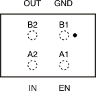
TPS72715, TPS72718, TPS72728, TPS72748
YFF Package
DSBGA-4
Top View
TPS727 po_yff_bvs128.gif
See note.
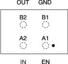
All Other TPS727 Devices
YFF Package
DSBGA-4
Top View
TPS727 po_yff_other_bvs128.gif
See note.
DSE Package
1,5mm × 1,5mm WSON-6
Top View
TPS727 po_dse_bvs128.gif
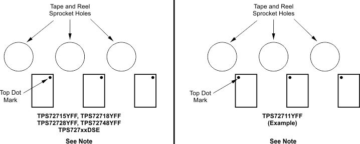
TPS727 dev_tape_reel_compare_bvs128.gif

NOTE

The EN pin is marked with a dot for the 1.5-V, 1.8-V, 2.8-V, and 4.8-V versions of the YFF package. The GND pin is marked with a dot for all other voltage versions of the YFF package. Refer to YFF0004 Package Outline page included at the end of this document for dimensions of the YFF package. On the package outline, the shaded box indicates the location of ball A1 and does not correlate to any marking on the topside of the physical package.
Pin Functions

PIN I/O DESCRIPTION
NAME YFF DSE
EN A1 4 I Enable pin. Driving EN over 0.9 V turns on the regulator. Driving EN below 0.4 V puts the regulator into shutdown mode, thus reducing the operating current to 120 nA, nominal.
GND B1 3 Ground pin.
IN A2 6 I Input pin. A small capacitor is needed from this pin to ground to assure stability. See in the Application Information section for more details.
NC 2, 5 No connection. This pin can be tied to ground to improve thermal dissipation.
OUT B2 1 O Regulated output voltage pin. A small 1-μF ceramic capacitor is needed from this pin to ground to assure stability. See in the Application Information section for more details.