SBVS263A July 2017 – September 2017 TPS7A39
PRODUCTION DATA.
- 1 Features
- 2 Applications
- 3 Description
- 4 Revision History
- 5 Pin Configuration and Functions
- 6 Specifications
- 7 Detailed Description
-
8 Application and Implementation
- 8.1
Application Information
- 8.1.1 Setting the Output Voltages on Adjustable Devices
- 8.1.2 Capacitor Recommendations
- 8.1.3 Input and Output Capacitor (CINx and COUTx)
- 8.1.4 Feed-Forward Capacitor (CFFx)
- 8.1.5 Noise-Reduction and Soft-Start Capacitor (CNR/SS)
- 8.1.6 Buffered Reference Voltage
- 8.1.7 Overriding Internal Reference
- 8.1.8 Start-Up
- 8.1.9 AC and Transient Performance
- 8.1.10 DC Performance
- 8.1.11 Reverse Current
- 8.1.12 Power Dissipation (PD)
- 8.2 Typical Applications
- 8.1
Application Information
- 9 Power-Supply Recommendations
- 10Layout
- 11Device and Documentation Support
- 12Mechanical, Packaging, and Orderable Information
8 Application and Implementation
NOTE
Information in the following applications sections is not part of the TI component specification, and TI does not warrant its accuracy or completeness. TI’s customers are responsible for determining suitability of components for their purposes. Customers should validate and test their design implementation to confirm system functionality.
8.1 Application Information
Successfully implementing an LDO in an application depends on the application requirements. This section discusses key device features and how to best implement the LDO to achieve a reliable design.
8.1.1 Setting the Output Voltages on Adjustable Devices
Figure 65 shows that each LDO resistor feedback network sets its output voltage. The positive LDO output voltage range is VNR/SS to 30 V and the negative LDO output voltage range is 0 V to –30 V.
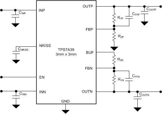 Figure 65. Adjustable Operation
Equation 1 relates the values of R1P and R2P to VOUTP(NOM) and VNR/SS to set the positive output voltage. Equation 2 relates the values of R1N and R2N to VOUTN(NOM) and VNR/SS to set the negative output voltage.
The positive LDO is configured as a noninverting op amp, whereas the negative LDO is an inverting op amp.
Substituting VNR/SS with VFBP on the positive channel and VNR/SS with VBUF on the negative channel gives a more accurate relationship.
Equation 3 and Equation 2 are rearranged versions of Equation 1 and Equation 2, with the above substitutions made.
The minimum bias current through both feedback networks is 5 µA to ensure accuracy.
For even tighter accuracy, take into account the input bias current into the error amplifiers (IFBP and IFBN) and use 0.1% resistors. Overriding the internal reference with a high accuracy external reference can also improve the accuracy of the device.
Table 4 and Table 5 show the resistor combinations for several common output voltages using commercially available, 1% tolerance resistors.
Table 4. Recommended Feedback-Resistor Values for the Positive LDO
| TARGETED OUTPUT VOLTAGE (V) | FEEDBACK RESISTOR VALUES(1) | CALCULATED OUTPUT VOLTAGE (V) | |
|---|---|---|---|
| R1P (kΩ) | R2P (kΩ) | ||
| 1.5 | 2.67 | 10.0 | 1.50 |
| 1.8 | 5.23 | 10.0 | 1.80 |
| 2.5 | 11.0 | 10.0 | 2.49 |
| 3.0 | 15.4 | 10.0 | 3.00 |
| 3.3 | 17.8 | 10.0 | 3.29 |
| 5.0 | 32.4 | 10.0 | 5.02 |
| 9.0 | 66.5 | 10.0 | 9.07 |
| 12.0 | 90.9 | 10.0 | 12.0 |
| 15.0 | 115 | 10.0 | 14.8 |
| 24.0 | 191 | 10.0 | 23.8 |
| 30.0 | 243 | 10.0 | 29.8 |
Table 5. Recommended Feedback-Resistor Values for the Negative LDO
| TARGETED OUTPUT VOLTAGE (V) | FEEDBACK RESISTOR VALUES(1) | CALCULATED OUTPUT VOLTAGE (V) | |
|---|---|---|---|
| R1N (kΩ) | R2N (kΩ) | ||
| -0.3 | 2.55 | 10.0 | -0.303 |
| -1.5 | 12.7 | 10.0 | -1.51 |
| -1.8 | 15.0 | 10.0 | -1.78 |
| -2.5 | 21.0 | 10.0 | -2.49 |
| -3.0 | 25.5 | 10.0 | -3.03 |
| -3.3 | 28.0 | 10.0 | -3.33 |
| -5.0 | 42.2 | 10.0 | -5.04 |
| -9.0 | 75.0 | 10.0 | -8.91 |
| -12.0 | 100 | 10.0 | -11.9 |
| -15.0 | 127 | 10.0 | -15.1 |
| -24.0 | 200 | 10.0 | -23.8 |
| -30.0 | 255 | 10.0 | -30.3 |
8.1.2 Capacitor Recommendations
The device is designed to be stable using low equivalent series resistance (ESR) ceramic capacitors at the input and output pins. The device is also designed to be stable with aluminum polymer and tantalum polymer capacitors with ESR < 75 mΩ.
Electrolytic capacitors (along with higher ESR polymer capacitors) can also be used if capacitors (meeting the minimum capacitance and ESR requirements ) are used in parallel.
Take the effective ESR for stability when the impedance of the capacitor is at its minimum. At the minimum level, the capacitance and parasitic inductance cancel each other and provides the DC ESR.
Ceramic capacitors that employ X7R-, X5R-, and COG-rated dielectric materials provide relatively good capacitive stability across temperature, whereas the use of Y5V-rated capacitors is discouraged because of large variations in capacitance.
Regardless of the ceramic capacitor type selected, ceramic capacitance varies with operating voltage and temperature. As a rule of thumb, derate ceramic capacitors by at least 50%. The input and output capacitors recommended herein account for an effective capacitance derating of approximately 50%, but at higher VIN and VOUT conditions (that is, VIN = 5.5 V to VOUT = 5.0 V) the derating can be greater than 50% and must be taken into consideration.
For high performance applications polymer capacitors are ideal as they do not experience the large deratings of ceramic capacitors.
8.1.3 Input and Output Capacitor (CINx and COUTx)
The device is designed and characterized for operation with ceramic capacitors of 10 µF or greater (2.2 µF or greater of effective capacitance) at each input and output.
Locate the input and output capacitors as near as practical to the respective input and output pins to minimize the trace inductance from the capacitor to the device. If the LDO is used to produce low output voltages (below 5 V), a 4.7-µF output capacitor can be used. If a 4.7-µF output capacitor is used, be sure to account for the derating of the capacitors during design.
Large, fast line transients on the input supplies can cause the device output to momentarily turn off. Typically these transients do not occur in most applications, but when these transients do occur use a larger input capacitor to slow down the line transient. If the system has input line transients that are faster than 0.5 V/µs, increase the input capacitance.
8.1.4 Feed-Forward Capacitor (CFFx)
Although a feed-forward capacitor (CFFx) from the FBx pin to the OUTx pin is not required to achieve stability, a 10-nF external CFFx capacitor optimizes the transient, noise, and PSRR performance. The maximum recommended value for CFFx is 100 nF.
A larger CFFx can dominate the start-up time set by CNR/SS, for more information see the Pros and Cons of Using a Feed-Forward Capacitor with a Low Dropout Regulator application report.
8.1.5 Noise-Reduction and Soft-Start Capacitor (CNR/SS)
Although a noise-reduction and soft-start capacitor (CNR/SS) from the NR/SS pin to GND is not required, CNR/SS is highly recommended to control the start-up time and reduce the noise-floor of the device. For start-up tracking to function correctly, a minimum 4.7-nF capacitor is required. As the time constant formed by the feedback resistors and feed-forward capacitors increases, the value of the CNR/SS capacitor must also be increased for startup tracking to work correctly. To figure out how to calculate the time constant of the feedback network see the Pros and Cons of Using a Feed-Forward Capacitor with a Low Dropout Regulator application report.
8.1.6 Buffered Reference Voltage
The voltage at the NR/SS pin, whether driven internally or externally, is buffered with a high-bandwidth, low-noise op amp. The BUF pin can be used as a voltage reference in many signal chain applications.
8.1.7 Overriding Internal Reference
The internal reference of the LDO can be overridden using an external source to increase the accuracy of the LDO and lower the output noise. To override the internal reference connect the external source to the NR/SS pin of the LDO. In order to overdrive the internal reference the external source must be able to source or sink 100 µA or greater.
The internal reference achieves a 2% accuracy from –40°C to +125°C; using an external reference can help achieve better accuracy over temperature.
8.1.8 Start-Up
8.1.8.1 Soft-Start Control (NR/SS)
Each output of the device features a user-adjustable, monotonic, voltage-controlled soft-start that is set with an external capacitor (CNR/SS). This soft-start eliminates power-up initialization problems.
The output voltage (VOUTx) rises proportionally to VNR/SS during start-up. As such, the time required for VNR/SS to reach its nominal value determines the rise time of VOUTx (start-up time).
The soft-start ramp time depends on the soft-start charging current (INR/SS), the soft-start capacitance (CNR/SS), and the internal reference (VNR/SS). Equation 5 calculates the approximate soft-start ramp time (tSS):
Values for the soft-start charging currents, RNR/SS, and the device internal CNR/SS are provided in the table.
8.1.8.1.1 In-Rush Current
In-rush current is defined as the current into the LDO at the INx pin during start-up. In-rush current then consists primarily of the sum of load current and the current used to charge the output capacitor. This current is difficult to measure because the input capacitor must be removed, which is not recommended. However, the in-rush current can be estimated by Equation 6:

where
- VOUTx(t) is the instantaneous output voltage of the turn-on ramp
- dVOUTx(t) / dt is the slope of the VOUTx ramp
- RLOAD is the resistive load impedance
8.1.8.2 Undervoltage Lockout (UVLOx) Control
The UVLOx circuit ensures that the device stays disabled before its input or bias supplies reach the minimum operational voltage range, and ensures that the device properly shuts down when the input supply collapses.
Figure 66 and Table 6 explain the UVLOx circuit response to various input voltage events, assuming VEN ≥ VIH(EN).
The positive and negative UVLO circuits are internally ANDed together. As such, if either supply collapses, both outputs turn-off and VNR/SS is pulled low internally.
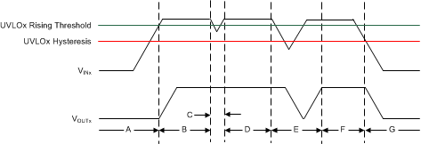 Figure 66. Typical UVLOx Operation
Table 6. Typical UVLOx Operation Description
| REGION | EVENT | VOUTx STATUS | COMMENT |
|---|---|---|---|
| A | Turn-on, |VINx| ≤ |VUVLOx| | 0 | Start-up |
| B | Regulation | 1 | Regulates to target VOUTx |
| C | Brownout,|VINx| ≥ |VUVLOx – VHYSx| | 1 | The output can fall out of regulation but the device is still enabled |
| D | Regulation | 1 | Regulates to target VOUTx |
| E | Brownout, |VINx| < |VUVLOx – VHYSx| | 0 | The device is disabled and the output falls because of the load and active discharge circuit. The device is reenabled when the UVLOx rising threshold is reached by the input voltage and a normal start-up then follows. |
| F | Regulation | 1 | Regulates to target VOUTx |
| G | Turn-off, |VINx| < |VUVLOx – VHYSx| | 0 | The output falls because of the load and active discharge circuit |
Similar to many other LDOs with this feature, the UVLOx circuit takes a few microseconds to fully assert. During this time, a downward line transient below approximately 0.8 V causes the UVLOx to assert for a short time; however, the UVLOx circuit does not have enough stored energy to fully discharge the internal circuits inside of the device. When the UVLOx circuit is not given enough time to fully discharge the internal nodes, the outputs are not fully disabled.
The effect of the downward line transient can be mitigated by using a larger input capacitor to increase the fall time of the input supply when operating near the minimum VINx.
8.1.9 AC and Transient Performance
LDO ac performance for a dual-channel device includes power-supply rejection ratio, channel-to-channel output isolation, output current transient response, and output noise. These metrics are primarily a function of open-loop gain, bandwidth, and phase margin that control the closed-loop input and output impedance of the LDO. The output noise is primarily a result of the band-gap reference and error amplifier noise.
8.1.9.1 Power-Supply Rejection Ratio (PSRR)
PSRR is a measure of how well the LDO control-loop rejects signals from VINx to VOUTx across the frequency spectrum (usually 10 Hz to 10 MHz). Equation 7 gives the PSRR calculation as a function of frequency for the input signal [VINx(f)] and output signal [VOUTx(f)].

Even though PSRR is a loss in signal amplitude, PSRR is shown as positive values in decibels (dB) for convenience.
Figure 67 shows a simplified diagram of PSRR versus frequency.
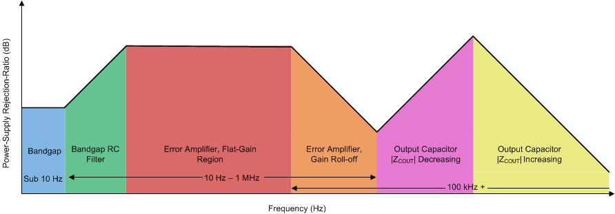 Figure 67. Power-Supply Rejection Ratio Diagram
An LDO is often employed not only as a dc-dc regulator, but also to provide exceptionally clean power-supply voltages that exhibit ultra-low noise and ripple to sensitive system components.
8.1.9.2 Channel-to-Channel Output Isolation and Crosstalk
Output isolation is a measure of how well the device prevents voltage disturbances on one output from affecting the other output. This attenuation appears in load transient tests on the other output; however, to numerically quantify the rejection, the output channel isolation is expressed in decibels (dB).
Output isolation performance is a strong function of the PCB layout. See the Layout Guidelines section on how to best optimize the isolation performance.
8.1.9.3 Output Voltage Noise
The TPS7A39 is designed for system applications where minimizing noise on the power-supply rail is critical to system performance. For example, the TPS7A39 can be used in a phase-locked loop (PLL)-based clocking circuit that can be used for minimum phase noise, or in test and measurement systems where even small power-supply noise fluctuations reduce system dynamic range.
LDO noise is defined as the internally-generated intrinsic noise created by the semiconductor circuits alone. This noise is the sum of various types of noise (such as shot noise associated with current-through-pin junctions, thermal noise caused by thermal agitation of charge carriers, flicker noise, or 1/f noise and dominates at lower frequencies as a function of 1/f). Figure 68 shows a simplified output voltage noise density plot versus frequency.
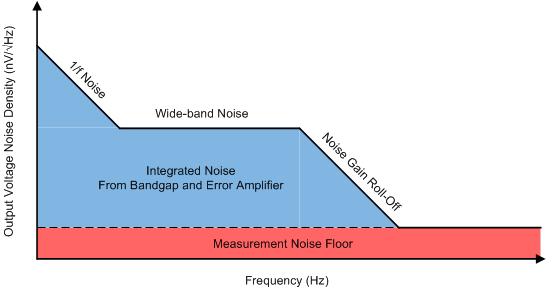 Figure 68. Output Voltage Noise Diagram
For further details, see the How to Measure LDO Noise white paper.
8.1.9.4 Optimizing Noise and PSRR
Table 7 describes how the ultra-low noise floor and PSRR of the device can be improved in several ways.
Table 7. Effect of Various Parameters on AC Performance(1)(2)
| PARAMETER | NOISE | PSRR | ||||
|---|---|---|---|---|---|---|
| LOW-FREQUENCY | MID-FREQUENCY | HIGH-FREQUENCY | LOW-FREQUENCY | MID-FREQUENCY | HIGH-FREQUENCY | |
| CNR/SS | +++ | No effect | No effect | +++ | + | No effect |
| CFFx | ++ | +++ | + | ++ | +++ | + |
| COUTx | No effect | + | +++ | No effect | + | +++ |
| |VINx| – |VOUTx| | + | + | + | +++ | +++ | ++ |
| PCB layout | ++ | ++ | + | + | +++ | +++ |
The noise-reduction capacitor, in conjunction with the noise-reduction resistor, forms a low-pass filter (LPF) that filters out the noise from the reference before being gained up with the error amplifier, thereby minimizing the output voltage noise floor. The LPF is a single-pole filter and the cutoff frequency can be calculated with Equation 8. The effect of the CNR/SS capacitor increases when VOUTx(NOM) increases because the noise from the reference is gained up when the output voltage increases. For low-noise applications, a 10-nF to 1-µF CNR/SS is recommended.
The feed-forward capacitor reduces output voltage noise by filtering out the mid-band frequency noise. The feed-forward capacitor can be optimized by placing a pole-zero pair near the edge of the loop bandwidth and pushing out the loop bandwidth, thus improving mid-band PSRR.
A larger COUTx or multiple output capacitors reduces high-frequency output voltage noise and PSRR by reducing the high-frequency output impedance of the power supply.
Additionally, a higher input voltage improves the noise and PSRR because greater headroom is provided for the internal circuits. However, a high power dissipation across the die increases the output noise because of the increase in junction temperature.
Good PCB layout improves the PSRR and noise performance by providing heatsinking at low frequencies and isolating VOUTx at high frequencies.
8.1.9.5 Load Transient Response
The load-step transient response is the output voltage response by the LDO to a step in load current, whereby output voltage regulation is maintained. There are two key transitions during a load transient response: the transition from a light to a heavy load and the transition from a heavy to a light load. The regions illustrated in Figure 69 are broken down in this section and are described in Table 8. Regions A, E, and H are where the output voltage is in steady-state. Increasing the output capacitance improves the transient response (less dip); however, the transient takes longer to recover when using a large output capacitor.
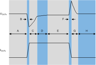 Figure 69. Load Transient Waveform
Table 8. Load Transient Waveform Description
| REGION | DESCRIPTION | COMMENT |
|---|---|---|
| A | Regulation | Regulation |
| B | Output current ramping | Initial voltage dip is a result of the depletion of the output capacitor charge. |
| C | LDO responding to transient | Recovery from the dip results from the LDO increasing its sourcing current, and leads to output voltage regulation. |
| D | Reaching thermal equilibrium | At high load currents the LDO takes some time to heat up. During this time the output voltage changes slightly. |
| E | Regulation | Regulation |
| F | Output current ramping | Initial voltage rise results from the LDO sourcing a large current, and leads to the output capacitor charge to increase. |
| G | LDO responding to transient | Recovery from the rise results from the LDO decreasing its sourcing current in combination with the load discharging the output capacitor. |
| H | Regulation | Regulation |
8.1.10 DC Performance
8.1.10.1 Output Voltage Accuracy (VOUTx)
The device features an output voltage accuracy that includes the errors introduced by the internal reference, load regulation, line regulation, process variation, and operating temperature as specified by the table. Output voltage accuracy specifies minimum and maximum output voltage error, relative to the expected nominal output voltage stated as a percent (for very low output voltages this specification is in mV).
8.1.10.2 Dropout Voltage (VDO)
Generally speaking, the dropout voltage often refers to the minimum voltage difference between the input and output voltage (|VDO| = |VINx| – |VOUTx|) that is required for regulation. When VINx drops below the required VDOx for the given load current, the device functions as a resistive switch and does not regulate output voltage. Dropout voltage is proportional to the output current because the device is operating as a resistive switch.
8.1.11 Reverse Current
As with most LDOs, this device can be damaged by excessive reverse current.
Reverse current is current that flows through the substrate of the device instead of the normal conducting channel of the pass element. This current flow, at high enough magnitudes, degrades long-term reliability of the device resulting from risks of electromigration and excess heat being dissipated across the device.
Conditions where excessive reverse current can occur are outlined in this section, all of which can exceed the absolute maximum rating of VOUTP > VINP + 0.3 V and VOUTN < VINN – 0.3 V:
- If the device has a large COUTx and the input supply collapses quickly with little or no load current
- The output is biased when the input supply is not established
- The output is biased above the input supply
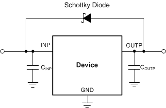 Figure 70. Example Circuit for Reverse Current Protection Using a Schottky Diode On Positive Rail
8.1.12 Power Dissipation (PD)
Circuit reliability demands that proper consideration is given to device power dissipation, location of the circuit on the printed circuit board (PCB), and correct sizing of the thermal plane. The PCB area around the regulator must be as free as possible of other heat-generating devices that cause added thermal stresses.
As a first-order approximation, power dissipation in the regulator depends on the input-to-output voltage difference and load conditions. Use Equation 9 to approximate PD:
Careful selection of the system voltage rails minimizes power dissipation and improves system efficiency. Proper selection allows the minimum input-to-output voltage differential to be obtained. The low dropout of the device allows for maximum efficiency across a wide range of output voltages.
The main heat conduction path for the device is through the thermal pad on the package. As such, the thermal pad must be soldered to a copper pad area under the device. This pad area contains an array of plated vias that conduct heat to any inner plane areas or to a bottom-side copper plane.
The maximum power dissipation determines the maximum allowable junction temperature (TJ) for the device. According to Equation 10, power dissipation and junction temperature are most often related by the junction-to-ambient thermal resistance (θJA) of the combined PCB, device package, and the temperature of the ambient air (TA).
Unfortunately, this thermal resistance (θJA) is highly dependent on the heat-spreading capability built into the particular PCB design, and therefore varies according to the total copper area, copper weight, and location of the planes. The θJA recorded in the Electrical Characteristics table is determined by the JEDEC standard, PCB, and copper-spreading area, and is only used as a relative measure of package thermal performance. For a well-designed thermal layout, θJA is actually the sum of the WSON package junction-to-case (bottom) thermal resistance (θJCbot) plus the thermal resistance contribution by the PCB copper.
8.1.12.1 Estimating Junction Temperature
The JEDEC standard recommends the use of psi (Ψ) thermal metrics to estimate the junction temperatures of the LDO when in-circuit on a typical PCB board application. These metrics are not strictly speaking thermal resistances, but rather offer practical and relative means of estimating junction temperatures. These psi metrics are determined to be significantly independent of the copper-spreading area. The key thermal metrics (ΨJT and ΨJB) are given in the Electrical Characteristics table and are used in accordance with Equation 11.

where
- PD is the power dissipated as explained in Equation 9
- TT is the temperature at the center-top of the device package
- TB is the PCB surface temperature measured 1 mm from the device package and centered on the package edge
8.2 Typical Applications
8.2.1 Design 1: Single-Ended to Differential Isolated Supply
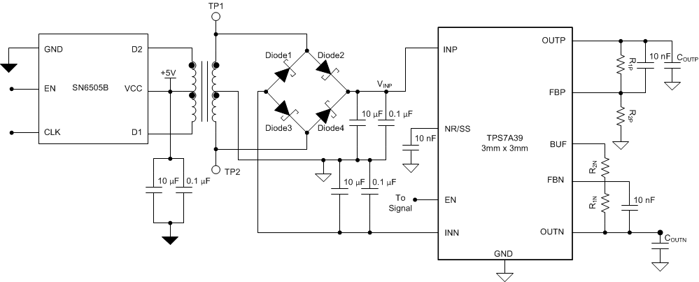 Figure 71. Single-Ended to Differential Isolated Supply Schematic
8.2.1.1 Design Requirements
Table 9. Design Requirements
| PARAMETER | DESIGN REQUIREMENT | DESIGN RESULT |
|---|---|---|
| Input supply | Must operate off of 5-V input | 5-V input supply |
| Output supply | Must have a 5-V and –5-V output | ±5-V output, ±2% accuracy |
| Positive output current | Capable of sourcing 50 mA on positive output | 50 mA (sourcing) |
| Negative output current | Capable of sinking 50 mA on negative output | 50 mA (sinking) |
| Isolation from 5-V supply | Must be isolated from input supply | Isolated through center tapped transformer |
| Efficiency | Must have > 80% efficiency at 100 mA(1) | 85% efficiency when IOUTN = –50 mA and IOUTP = 50 mA |
8.2.1.2 Detailed Design Procedure
8.2.1.2.1 Switcher Choice
This design incorporates a push-pull driver for center-tapped transformers that takes a single-ended supply and converts the supply to an isolated split rail design. The SN6505B provides a simple small-form factor isolated supply. The input voltage of the SN6505B can vary from 2.25 V to 5 V, which allows for use with a wide range of input supplies. The output voltage can be adjusted through the turns ratio of the transformer. Based on the choice of the transformer this design can be used to create output voltages from ±3.3 V to ±15 V. In this design the SN6505B was paired with the 750315371 center-tapped transformer from Wurth Electronics™. This transformer has a turns ratio of 1:1.1 and an isolation rating of 2500 VRMS (the total system isolation was never tested).
8.2.1.2.2 Full Bridge Rectifier With Center-Tapped Transformer
To create the isolated supply, the SN6505B uses a center-tapped transformer. A full bridge rectifier and capacitors are required to regulate the signal before reaching the LDO because of the alternating nature of the input signal. TI recommends having a fast switching and low forward voltage diode to improve efficiency because of how fast the SN6505 switches; Schottky diodes work well. Figure 73 shows the switching nodes of the SN6505 D1 and D2 and also shows where the transformer connects to the full bridge rectifier TP1 and TP2. Figure 73 shows the switching waveforms across the rectifier diodes.
 Figure 72. Bridge Rectifier With Center-Tapped Secondary Enables Bipolar Outputs
8.2.1.2.3 Total Solution Efficiency
Equation 12 shows how the efficiency of the system can be measured by taking the output power and dividing by the input power. IOUTP = |IOUTN| = IOUT / 2 because this system has two output rails to simplify the efficiency measurement. When the necessary parameters are measured, and by using Equation 12, the overall system efficiency can be plotted as in Figure 74. Figure 74 shows the overall system efficiency for this design, at the maximum output current of 100 mA (IOUTP = 50 mA, IOUTN = –50 mA) the efficiency of the system is 85%.
8.2.1.2.4 Feedback Resistor Selection
Equation 13 and Equation 14 calculate the values of the feedback resistors.
For this design the recommended 10-kΩ resistors are used for R2P and R2N. R1P and R1N can be calculated by substituting R2P and R2N into Equation 15 and Equation 16 because R2P and R2N are already selected
After solving for Equation 15 and Equation 16, the closest one percent resistors are selected, R1N = 42.2 kΩ and R1P = 32.4 kΩ.
8.2.1.3 Application Curves

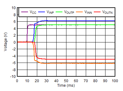
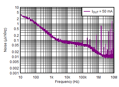

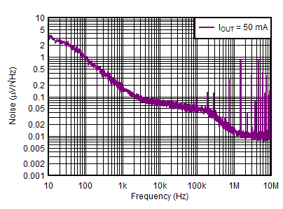
| IOUT = IOUTP + |IOUTN|, IOUTP = |IOUTN| |
8.2.2 Design 2: Getting the Full Range of a SAR ADC
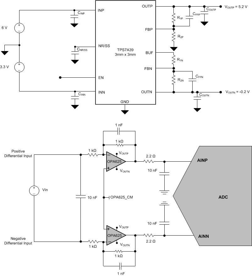 Figure 78. Creating Power Rails for an Analog Front-End of an ADC
8.2.2.1 Design Requirements
A common problem in analog-to-digital converters (ADCs) is that as the input signal approaches the edge of the range of the ADC, the signal begins to become distorted. Often times this is not because of a limitation of the ADC, but is a result of the analog front-end (AFE). In the AFE, the signal begins to approach the rails of the op amp and the signal begins to lose linearity and becomes distorted. This distortion is because when the rail-to-rail op amp begins to enter the nonlinear region of operation within 100 mV of the rail, the signal-to-noise ratio (SNR) starts to degrade and the total harmonic distortion (THD) of the ADC increases. To prevent the op amp from exiting the linear region of operation, the design must use a power supply that can generate rails 200 mV above and below the input range of the ADC.
8.2.2.2 Detailed Design Procedure
In this design, the ADS8900B is used as the ADC. This ADC features a differential input, so from a 5-V reference the ADC is able to encode values between ±5 V. In many applications, single-supply op amps are powered with rails from 0 V to 5 V, which causes the input signal to become distorted when the full range signal is applied. The FFT of a 10-VPP (peak-to-peak) sine wave using a single 5-V rail to bias the amplifiers is illustrated in Figure 79. In this test the SNR was calculated to be 54.89 dB and the THD was calculated to be –40.68 dB.
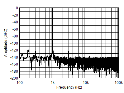
There is a simple solution to improve the SNR and THD of the ADC: bias the amplifiers in the analog front end with a 5.2-V rail and a –0.2-V rail. Using these rails allows the amplifier to operate in the linear region in the 0-V to 5-V range needed by the ADC. The FFT of a 10-VPP sine wave using a 5.2-V rail and a –0.2-V rail is illustrated in Figure 80. In this test the SNR was calculated to be 102.535 dB and the THD was calculated to be –121.66 dB. Using –0.2-V and 5.2-V rail voltages still allows for common 5-V (5.5 V max) op amps to be used in the design.
8.2.2.3 Detailed Design Description
8.2.2.3.1 Regulation of –0.2 V
The TPS7A39 has an innovative feature of regulating the negative rail down to zero volts. This regulation is achieved by using an inverting amplifier and using the positive-buffered reference as the input signal to the amplifier. Regulating to –0.2 V eliminates the nonlinearity and distortion present when using the full rail range of the amplifiers.
8.2.2.3.2 Feedback Resistor Selection
Use Equation 17 and Equation 18 to calculate the values of the feedback resistors:
For this design the recommended 10-kΩ resistors are used for R2P and R2N. R1P and R1N can be calculated by substituting R2P and R2N into Equation 19 and Equation 20 because R2P and R2N are already selected.
After solving for Equation 19 and Equation 20, the closest one percent resistors are selected, R1N = 1.69 kΩ and R1P = 34 kΩ.
8.2.2.4 Application Curves
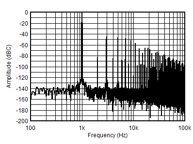
| fIN = 1 kHz, VPP = 10.0 V |
| fIN = 1 kHz, VPP = 10.0 V |