SBVS267A January 2016 – February 2016 TPS7A85
PRODUCTION DATA.
- 1 Features
- 2 Applications
- 3 Description
- 4 Revision History
- 5 Pin Configurations and Functions
- 6 Specifications
- 7 Detailed Description
-
8 Application and Implementation
- 8.1
Application Information
- 8.1.1 Recommended Capacitor Types
- 8.1.2 Input and Output Capacitor Requirements (CIN and COUT)
- 8.1.3 Noise-Reduction and Soft-Start Capacitor (CNR/SS)
- 8.1.4 Feed-Forward Capacitor (CFF)
- 8.1.5 Soft-Start and In-Rush Current
- 8.1.6 Optimizing Noise and PSRR
- 8.1.7 ANY-OUT Programmable Output Voltage
- 8.1.8 ANY-OUT Operation
- 8.1.9 Increasing ANY-OUT Resolution for LILO Conditions
- 8.1.10 Current Sharing
- 8.1.11 Adjustable Operation
- 8.1.12 Sequencing Requirements
- 8.1.13 Power-Good (PG) Operation
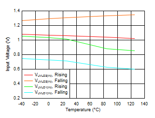
- 8.1.14 Undervoltage Lockout (UVLO) Operation
- 8.1.15 Dropout Voltage (VDO)
- 8.1.16 Behavior when Transitioning from Dropout into Regulation
- 8.1.17 Load Transient Response
- 8.1.18 Negatively-Biased Output
- 8.1.19 Reverse Current Protection
- 8.1.20 Power Dissipation (PD)
- 8.2 Typical Applications
- 8.1
Application Information
- 9 Power-Supply Recommendations
- 10Layout
- 11Device and Documentation Support
- 12Mechanical, Packaging, and Orderable Information
6 Specifications
6.1 Absolute Maximum Ratings
over junction temperature range (unless otherwise noted)(1)| MIN | MAX | UNIT | ||
|---|---|---|---|---|
| Voltage | IN, BIAS, PG, EN | –0.3 | 7.0 | V |
| IN, BIAS, PG, EN (5% duty cycle, pulse duration = 200 µs) | –0.3 | 7.5 | ||
| SNS, OUT | –0.3 | VIN + 0.3(2) | ||
| NR/SS, FB | –0.3 | 3.6 | ||
| 50mV, 100mV, 200mV, 400mV, 800mV, 1.6V | –0.3 | VOUT + 0.3 | ||
| Current | OUT | Internally limited | A | |
| PG (sink current into device) | 5 | mA | ||
| Operating junction temperature, TJ | –55 | 150 | °C | |
| Storage temperature, Tstg | –55 | 150 | °C | |
(1) Stresses beyond those listed under Absolute Maximum Ratings may cause permanent damage to the device. These are stress ratings only, which do not imply functional operation of the device at these or any other conditions beyond those indicated under Recommended Operating Conditions. Exposure to absolute-maximum-rated conditions for extended periods may affect device reliability.
(2) The absolute maximum rating is VIN + 0.3 V or 7.0 V, whichever is smaller.
6.2 ESD Ratings
| VALUE | UNIT | |||
|---|---|---|---|---|
| V(ESD) | Electrostatic discharge | Human-body model (HBM), per ANSI/ESDA/JEDEC JS-001(1) | ±2000 | V |
| Charged-device model (CDM), per JEDEC specification JESD22-C101(2) | ±500 | |||
(1) JEDEC document JEP155 states that 500-V HBM allows safe manufacturing with a standard ESD control process.
(2) JEDEC document JEP157 states that 250-V CDM allows safe manufacturing with a standard ESD control process.
6.3 Recommended Operating Conditions
over junction temperature range (unless otherwise noted)| MIN | NOM | MAX | UNIT | ||
|---|---|---|---|---|---|
| VIN | Input supply voltage range | 1.1 | 6.5 | V | |
| VBIAS | Bias supply voltage range(1) | 3.0 | 6.5 | V | |
| VOUT | Output voltage range(2) | 0.8 | 5 | V | |
| VEN | Enable voltage range | 0 | VIN | V | |
| IOUT | Output current | 0 | 4 | A | |
| CIN | Input capacitor | 10 | 47 | µF | |
| COUT | Output capacitor | 47 | 47 || 10 || 10(3) | µF | |
| RPG | Power-good pullup resistance | 10 | 100 | kΩ | |
| CNR/SS | NR/SS capacitor | 10 | nF | ||
| CFF | Feed-forward capacitor | 10 | nF | ||
| R1 | Top resistor value in feedback network for adjustable operation | 12.1(4) | kΩ | ||
| R2 | Bottom resistor value in feedback network for adjustable operation | 160(5) | kΩ | ||
| TJ | Operating junction temperature | –40 | 125 | °C | |
(1) BIAS supply is required when the VIN supply is below 1.4 V. Conversely, no BIAS supply is required when the VIN supply is higher than or equal to 1.4 V. A BIAS supply helps improve dc and ac performance for VIN ≤ 2.2 V.
(2) This output voltage range does not include device accuracy or accuracy of the feedback resistors.
(3) The recommended output capacitors are selected to optimize PSRR for the frequency range of 400 kHz to 700 kHz. This frequency range is a typical value for dc-dc supplies.
(4) The 12.1-kΩ resistor is selected to optimize PSRR and noise by matching the internal R1 value.
(5) The upper limit for the R2 resistor is to ensure accuracy by making the current through the feedback network much larger than the leakage current into the feedback node.
6.4 Thermal Information
| THERMAL METRIC(1) | TPS7A85 | UNIT | |
|---|---|---|---|
| RGR (VQFN) | |||
| 20 PINS | |||
| RθJA | Junction-to-ambient thermal resistance | 35.4 | °C/W |
| RθJC(top) | Junction-to-case (top) thermal resistance | 47.6 | °C/W |
| RθJB | Junction-to-board thermal resistance | 12.3 | °C/W |
| ψJT | Junction-to-top characterization parameter | 0.5 | °C/W |
| ψJB | Junction-to-board characterization parameter | 12.4 | °C/W |
| RθJC(bot) | Junction-to-case (bottom) thermal resistance | 1.0 | °C/W |
(1) For more information about traditional and new thermal metrics, see the IC Package Thermal Metrics application report, SPRA953.
6.5 Electrical Characteristics
Over operating junction temperature range (TJ = –40°C to +125°C), VIN = 1.4 V or VIN = VOUT(nom) + 0.5 V (whichever is greater), VBIAS = open, VOUT(nom) = 0.8 V(2), OUT connected to 50 Ω to GND(3), VEN = 1.1 V, CIN = 10 μF, COUT = 47 μF, CNR/SS without CFF, and PG pin pulled up to VIN with 100 kΩ, unless otherwise noted. Typical values are at TJ = 25°C.| PARAMETER | TEST CONDITIONS | MIN | TYP | MAX | UNIT | |||
|---|---|---|---|---|---|---|---|---|
| VIN | Input supply voltage range(1) | 1.1 | 6.5 | V | ||||
| VBIAS | Bias supply voltage range(1) | VIN = 1.1 V | 3.0 | 6.5 | V | |||
| VFB | Feedback voltage | 0.8 | V | |||||
| VNR/SS | NR/SS pin voltage | 0.8 | V | |||||
| VUVLO1(IN) | Input supply UVLO with BIAS | VIN rising with VBIAS = 3.0 V | 1.02 | 1.085 | V | |||
| VHYS1(IN) | VUVLO1(IN) hysteresis | VBIAS = 3.0 V | 320 | mV | ||||
| VUVLO2(IN) | Input supply UVLO without BIAS | VIN rising | 1.31 | 1.39 | V | |||
| VHYS2(IN) | VUVLO2(IN) hysteresis | 253 | mV | |||||
| VUVLO(BIAS) | Bias supply UVLO | VBIAS rising, VIN = 1.1 V | 2.83 | 2.9 | V | |||
| VHYS(BIAS) | VUVLO(BIAS) hysteresis | VIN = 1.1 V | 290 | mV | ||||
| VOUT | Output voltage | Range | Using the ANY-OUT pins | 0.8 – 1.0% | 3.95 + 1.0% | V | ||
| Using external resistors(4) | 0.8 – 1.0% | 5.0 + 1.0% | ||||||
| Accuracy(4)(5) | 0.8 V ≤ VOUT ≤ 5 V, 5 mA ≤ IOUT ≤ 4 A, over VIN | –1.0% | 1.0% | |||||
| Accuracy with BIAS | VIN = 1.1 V, 5 mA ≤ IOUT ≤ 4 A, 3.0 V ≤ VBIAS ≤ 6.5 V |
–0.75% | 0.75% | |||||
| ΔVOUT/ ΔVIN |
Line regulation | IOUT = 5 mA, 1.4 V ≤ VIN ≤ 6.5 V | 0.0035 | mV/V | ||||
| ΔVOUT/ ΔIOUT |
Load regulation | 5 mA ≤ IOUT ≤ 4 A, 3.0 V ≤ VBIAS ≤ 6.5 V, VIN = 1.1 V |
0.07 | mV/A | ||||
| 5 mA ≤ IOUT ≤ 4 A | 0.08 | |||||||
| 5 mA ≤ IOUT ≤ 4 A, VOUT = 5.0 V | 0.4 | |||||||
| VDO | Dropout voltage | VIN = 1.4 V, IOUT = 4 A, VFB = 0.8 V – 3% | 215 | 320 | mV | |||
| VIN = 5.5 V, IOUT = 4 A, VFB = 0.8 V – 3% | 325 | 500 | ||||||
| VIN = 1.1 V, VBIAS = 5.0 V, IOUT = 4 A, VFB = 0.8 V – 3% |
150 | 240 | ||||||
| ILIM | Output current limit | VOUT forced at 0.9 × VOUT(nom), VIN = VOUT(nom) + 0.4 V |
4.7 | 5.2 | 5.7 | A | ||
| ISC | Short-circuit current limit | RLOAD = 20 mΩ | 1.0 | A | ||||
| IGND | GND pin current | VIN = 6.5 V, IOUT = 5 mA | 2.8 | 4.0 | mA | |||
| VIN = 1.4 V, IOUT = 4 A | 4.8 | 6.0 | ||||||
| Shutdown, PG = open, VIN = 6.5 V, VEN = 0.5 V | 25 | µA | ||||||
| IEN | EN pin current | VIN = 6.5 V, VEN = 0 V and 6.5 V | –0.1 | 0.1 | µA | |||
| IBIAS | BIAS pin current | VIN = 1.1 V, VBIAS = 6.5 V, VOUT(nom) = 0.8 V, IOUT = 4 A |
2.3 | 3.5 | mA | |||
| VIL(EN) | EN pin high-level input voltage (enable device) |
0 | 0.5 | V | ||||
| VIH(EN) | EN pin low-level input voltage (disable device) |
1.1 | 6.5 | V | ||||
| VIT(PG) | PG pin threshold | For falling VOUT | 82% × VOUT | 88.3% × VOUT | 93% × VOUT | V | ||
| VHYS(PG) | PG pin hysteresis | For rising VOUT | 1% × VOUT | V | ||||
| VOL(PG) | PG pin low-level output voltage | VOUT < VIT(PG), IPG = –1 mA (current sunk into pin) |
0.4 | V | ||||
| Ilkg(PG) | PG pin leakage current | VOUT > VIT(PG), VPG = 6.5 V | 1 | µA | ||||
| INR/SS | NR/SS pin charging current | VNR/SS = GND, VIN = 6.5 V | 4.0 | 6.2 | 9.0 | µA | ||
| IFB | FB pin leakage current | VIN = 6.5 V | –100 | 100 | nA | |||
| PSRR | Power-supply ripple rejection | VIN – VOUT = 0.5 V, IOUT = 4 A, CNR/SS = 100 nF, CFF = 10 nF, COUT = 47 μF || 10 μF || 10 μF |
f = 10 kHz, VOUT = 0.8 V, VBIAS = 5.0 V |
42 | dB | |||
| f = 500 kHz, VOUT = 0.8 V, VBIAS = 5.0 V | 39 | |||||||
| f = 10 kHz, VOUT = 3.3 V |
40 | |||||||
| f = 500 kHz, VOUT = 3.3 V | 25 | |||||||
| Vn | Output noise voltage | BW = 10 Hz to 100 kHz, VIN = 1.2 V, VOUT = 0.8 V, VBIAS = 5.0 V, IOUT = 4 A, CNR/SS = 100 nF, CFF = 10 nF, COUT = 47 μF || 10 μF || 10 μF |
4.4 | μVRMS | ||||
| BW = 10 Hz to 100 kHz, VOUT = 5.0 V, IOUT = 4 A, CNR/SS = 100 nF, CFF = 10 nF, COUT = 47 μF || 10 μF || 10 μF |
8.4 | |||||||
| Tsd | Thermal shutdown temperature | Shutdown, temperature increasing | 160 | °C | ||||
| Reset, temperature decreasing | 140 | |||||||
| TJ | Operating junction temperature | –40 | 125 | °C | ||||
(1) BIAS supply is required when the VIN supply is below 1.4 V. Conversely, no BIAS supply is required when the VIN supply is higher than or equal to 1.4 V. A BIAS supply helps improve dc and ac performance for VIN ≤ 2.2 V.
(2) VOUT(nom) is the calculated VOUT target value from the ANY-OUT in a fixed configuration. In an adjustable configuration, VOUT(nom) is the expected VOUT value set by the external feedback resistors.
(3) This 50-Ω load is disconnected when the test conditions specify an IOUT value.
(4) When the device is connected to external feedback resistors at the FB pin, external resistor tolerances are not included.
(5) The device is not tested under conditions where VIN > VOUT + 1.25 V and IOUT = 4 A, because the power dissipation is higher than the maximum rating of the package.
6.6 Typical Characteristics
at TA = 25°C, VIN = 1.4 V or VIN = VOUT(NOM) + 0.5 V (whichever is greater), VBIAS = open, VOUT(NOM) = 0.8 V, VEN = 1.1 V, COUT = 47 μF, CNR/SS = 0 nF, CFF = 0 nF, and PG pin pulled up to VIN with 100 kΩ (unless otherwise noted)
| VIN = 1.2 V, VBIAS = 5 V, COUT = 47 μF || 10 μF || 10 μF, CNR/SS = 10 nF, CFF = 10 nF |

| VIN = 1.4 V, IOUT = 1 A, COUT = 47 μF || 10 μF || 10 μF, CNR/SS = 10 nF, CFF = 10 nF |

| VIN = VOUT + 0.4 V, VBIAS = 5.0 V, IOUT = 4 A, COUT = 47 μF || 10 μF || 10 μF, CNR/SS = 10 nF, CFF = 10 nF |

| VIN = 5.6 V, COUT = 47 μF || 10 μF || 10 μF, CNR/SS = 10 nF, CFF = 10 nF |
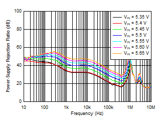
| IOUT = 4 A, COUT = 47 μF || 10 μF || 10 μF, CNR/SS = 10 nF, CFF = 10 nF |
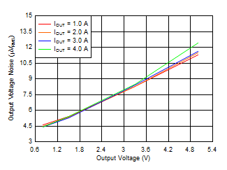
| VIN = VOUT + 0.4 V and VBIAS = 5 V for VOUT ≤ 2.2 V,
COUT = 47 μF || 10 μF || 10 μF, CNR/SS = 10 nF, CFF = 10 nF |

| IOUT = 1 A, COUT = 47 μF || 10 μF || 10 μF, CNR/SS = 10 nF, CFF = 10 nF |

| VIN = VOUT + 0.4 V, VBIAS = 5 V, IOUT = 4 A, COUT = 47 μF || 10 μF || 10 μF, CNR/SS = 10 nF |

| VIN = 1.2 V, VOUT = 0.9 V, VBIAS = 5.0 V, IOUT = 4 A, COUT = 47 μF || 10 μF || 10 μF, CFF = 10 nF |

| IOUT, DC = 100 mA, COUT = 47 μF || 10 μF || 10 μF, CNR/SS = CFF = 10 nF, slew rate = 1 A/μs |
VOUT without Bias
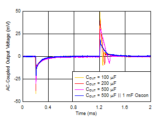
| VIN = 1.2 V, VBIAS = 5.0 V, IOUT = 100 mA to 4 A, CNR/SS = CFF = 10 nF, slew rate = 1 A/μs |
(VOUT = 0.9 V)

| IOUT = 4 A, VBIAS = 0 V |

| VIN = 1.4 V, VBIAS = 0 V |

| VIN = 5.5 V |


| VIN = 1.1 V, IOUT = 5 mA |

| IOUT = 5 mA |


| VIN = 1.1 V |


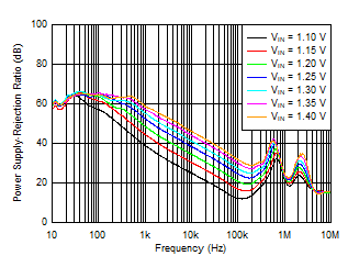
| IOUT = 4 A, VBIAS = 5 V, COUT = 47 μF || 10 μF || 10 μF, CNR/SS = 10 nF, CFF = 10 nF |

| IOUT = 1 A, COUT = 47 μF || 10 μF || 10 μF, CNR/SS = 10 nF, CFF = 10 nF |

| IOUT = 4 A, COUT = 47 μF || 10 μF || 10 μF, CNR/SS = 10 nF, CFF = 10 nF |
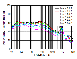
| VIN = VOUT + 0.4 V, VOUT = 1 V, IOUT = 4 A,
COUT = 47 μF || 10 μF || 10 μF, CNR/SS = 10 nF, CFF = 10 nF |
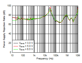
| VIN = VOUT + 0.4 V, VOUT = 1 V, IOUT = 4 A,
COUT = 47 μF || 10 μF || 10 μF, CNR/SS = 10 nF, CFF = 10 nF |

| VIN = VOUT + 0.4 V and VBIAS = 5 V for VOUT ≤ 2.2 V, IOUT = 4 A, COUT = 47 μF || 10 μF || 10 μF, CNR/SS = 10 nF, CFF = 10 nF |

| VIN = VOUT + 0.4 V, VBIAS = 5 V, IOUT = 4 A, COUT = 47 μF || 10 μF || 10 μF, CFF = 10 nF |
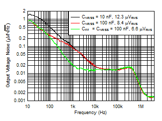
| VIN = 5.6 V, IOUT = 4 A, COUT = 47 μF || 10 μF || 10 μF, CFF = 10 nF |

| VIN = VOUT + 0.3 V, VBIAS = 5 V, IOUT, DC = 100 mA, slew rate = 1 A/μs, CNR/SS = CFF = 10 nF, COUT = 47 μF || 10 μF || 10 μF |
VOUT with Bias

| VOUT = 5 V, IOUT, DC = 100 mA, IOUT = 100 mA to 4 A, COUT = 47 μF || 10 μF || 10 μF, CNR/SS = CFF = 10 nF |
Slew Rate

| VIN = 1.2 V, VBIAS = 5.0 V, COUT = 47 μF || 10 μF || 10 μF, CNR/SS = CFF = 10 nF, slew rate = 1 A/μs |
(VOUT = 0.9 V)

| IOUT = 4 A, VBIAS = 6.5 V |

| VIN = 1.1 V, VBIAS = 3 V |

| IOUT = 100 mA to 4 A |


| IOUT = 5 mA |
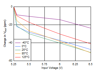
| IOUT = 5 mA |

| VIN = 1.1 V, IOUT = 5 mA |

| VIN = 1.1 V |


| VIN = 6.5 V |