SBVS291C April 2017 – December 2020 TPS7A84A
PRODUCTION DATA
- 1 Features
- 2 Applications
- 3 Description
- 4 Revision History
- 5 Pin Configuration and Functions
-
6 Specifications
- 6.1 Absolute Maximum Ratings
- 6.2 ESD Ratings
- 6.3 Recommended Operating Conditions
- 6.4 Thermal Information
- 6.5 Electrical Characteristics: General
- 6.6 Electrical Characteristics: TPS7A8400A
- 6.7 Electrical Characteristics: TPS7A8401A
- 6.8 Typical Characteristics: TPS7A8400A
- 6.9 Typical Characteristics: TPS7A8401A
- 7 Detailed Description
-
8 Application and Implementation
- 8.1
Application Information
- 8.1.1
External Component Selection
- 8.1.1.1 Adjustable Operation
- 8.1.1.2 ANY-OUT Programmable Output Voltage
- 8.1.1.3 ANY-OUT Operation
- 8.1.1.4 Increasing ANY-OUT Resolution for LILO Conditions
- 8.1.1.5 Current Sharing
- 8.1.1.6 Recommended Capacitor Types
- 8.1.1.7 Input and Output Capacitor Requirements (CIN and COUT)
- 8.1.1.8 Feed-Forward Capacitor (CFF)
- 8.1.1.9 Noise-Reduction and Soft-Start Capacitor (CNR/SS)
- 8.1.2 Start-Up
- 8.1.3 AC and Transient Performance
- 8.1.4 DC Performance
- 8.1.5 Sequencing Requirements
- 8.1.6 Negatively Biased Output
- 8.1.7 Reverse Current Protection
- 8.1.8 Power Dissipation (PD)
- 8.1.1
External Component Selection
- 8.2 Typical Applications
- 8.1
Application Information
- 9 Power Supply Recommendations
- 10Layout
- 11Device and Documentation Support
3 Description
The TPS7A84A is a low-noise, low-dropout linear regulator (LDO) capable of sourcing 3 A with only 180-mV of maximum dropout. The device is offered in two output voltage ranges. The TPS7A8400A output voltage is pin-programmable from 0.8 V to 3.95 V, with a 50-mV resolution, and adjustable from 0.8 V to 5.15 V using an external resistor divider. The TPS7A8401A output voltage is pin-programmable from 0.5 V to 2.075 V, with a 25-mV resolution, and adjustable from 0.5 V to 5.15 V using an external resistor divider.
The combination of low-noise,
high-PSRR, and high output-current capability makes the TPS7A84A ideal to power
noise-sensitive components such as those found in high-speed communications, video,
medical, or test and measurement applications. The high performance of the TPS7A84A
limits power-supply-generated phase noise and clock jitter, making this device ideal
for powering high-performance serializer and deserializer (SerDes),
analog-to-digital converters (ADCs), digital-to-analog converters (DACs), and RF
components. Specifically, RF amplifiers benefit from the high-performance and
> 5-V output capability of the device.
For digital loads [such as application-specific integrated circuits (ASICs), field-programmable gate arrays (FPGAs), and digital signal processors (DSPs)] requiring low-input voltage, low-output (LILO) voltage operation, the exceptional accuracy (0.75% over line, load, and temperature), remote sensing, excellent transient performance, and soft-start capabilities of the TPS7A84A ensure optimal system performance.
The versatility of the TPS7A84A makes the device a component of choice for many demanding applications.
| PART NUMBER | PACKAGE | BODY SIZE (NOM) |
|---|---|---|
| TPS7A84A | VQFN (20) | 3.50 mm × 3.50 mm |
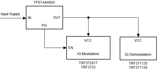
 Typical Application Diagram