SBVS291C April 2017 – December 2020 TPS7A84A
PRODUCTION DATA
- 1 Features
- 2 Applications
- 3 Description
- 4 Revision History
- 5 Pin Configuration and Functions
-
6 Specifications
- 6.1 Absolute Maximum Ratings
- 6.2 ESD Ratings
- 6.3 Recommended Operating Conditions
- 6.4 Thermal Information
- 6.5 Electrical Characteristics: General
- 6.6 Electrical Characteristics: TPS7A8400A
- 6.7 Electrical Characteristics: TPS7A8401A
- 6.8 Typical Characteristics: TPS7A8400A
- 6.9 Typical Characteristics: TPS7A8401A
- 7 Detailed Description
-
8 Application and Implementation
- 8.1
Application Information
- 8.1.1
External Component Selection
- 8.1.1.1 Adjustable Operation
- 8.1.1.2 ANY-OUT Programmable Output Voltage
- 8.1.1.3 ANY-OUT Operation
- 8.1.1.4 Increasing ANY-OUT Resolution for LILO Conditions
- 8.1.1.5 Current Sharing
- 8.1.1.6 Recommended Capacitor Types
- 8.1.1.7 Input and Output Capacitor Requirements (CIN and COUT)
- 8.1.1.8 Feed-Forward Capacitor (CFF)
- 8.1.1.9 Noise-Reduction and Soft-Start Capacitor (CNR/SS)
- 8.1.2 Start-Up
- 8.1.3 AC and Transient Performance
- 8.1.4 DC Performance
- 8.1.5 Sequencing Requirements
- 8.1.6 Negatively Biased Output
- 8.1.7 Reverse Current Protection
- 8.1.8 Power Dissipation (PD)
- 8.1.1
External Component Selection
- 8.2 Typical Applications
- 8.1
Application Information
- 9 Power Supply Recommendations
- 10Layout
- 11Device and Documentation Support
8.1.1.3 ANY-OUT Operation
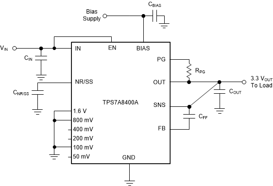
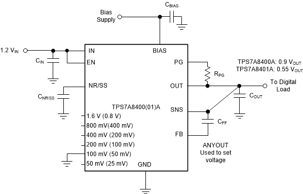
Considering the use of the ANY-OUT internal network (where the unit resistance of 1R, see , is equal to 6.05 kΩ) the output voltage is set by grounding the appropriate control pins, as shown in Figure 8-2. When grounded, all control pins add a specific voltage on top of the internal reference voltage (VNR/SS = 0.8 V). The output voltage can be calculated by Equation 4 and Equation 5. Figure 8-2 and Figure 8-3 show a 0.9-V output voltage, respectively, that provide an example of the circuit usage with and without bias voltage.
 Figure 8-2 ANY-OUT Configuration Circuit (TPS7A8400A) (3.3-V Output, No External Bias)
Equation 4. VOUT(nom) = VNR/SS + 1.6 V + 0.8 V + 0.1 V = 0.8 V + 1.6 V + 0.8 V + 0.1 V = 3.3 V
 Figure 8-3 ANY-OUT Configuration Circuit (0.9-V, 0.55-V Output with Bias)
Equation 5. VOUT(nom) = VNR/SS + 0.1 V = 0.8 V + 0.1 V = 0.9 V