SBVS295A November 2019 – March 2020 TPS7A52
PRODUCTION DATA.
- 1 Features
- 2 Applications
- 3 Description
- 4 Revision History
- 5 Pin Configuration and Functions
- 6 Specifications
- 7 Detailed Description
-
8 Application and Implementation
- 8.1
Application Information
- 8.1.1 Recommended Capacitor Types
- 8.1.2 Soft Start and Inrush Current
- 8.1.3 Optimizing Noise and PSRR
- 8.1.4 Charge Pump Noise
- 8.1.5 Current Sharing
- 8.1.6 Adjustable Operation
- 8.1.7 Power-Good Operation
- 8.1.8 Undervoltage Lockout (UVLO) Operation
- 8.1.9 Dropout Voltage (VDO)
- 8.1.10 Device Behavior During Transition From Dropout Into Regulation
- 8.1.11 Load Transient Response
- 8.1.12 Reverse Current Protection Considerations
- 8.1.13 Power Dissipation (PD)
- 8.1.14 Estimating Junction Temperature
- 8.1.15 TPS7A52EVM Thermal Analysis
- 8.2 Typical Application
- 8.1
Application Information
- 9 Power Supply Recommendations
- 10Layout
- 11Device and Documentation Support
- 12Mechanical, Packaging, and Orderable Information
7.3.1.1 DC Regulation
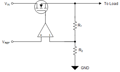
A low dropout regulator (LDO) functions as a class-B amplifier, as shown in Figure 26, in which the input signal is the internal reference voltage (VREF). VREF is designed to have very low bandwidth at the input to the error amplifier through the use of a low-pass filter (VNR/SS).
As such, the reference can be considered as a pure dc input signal. The low output impedance of an LDO comes from the combination of the output capacitor and pass element. The pass element also presents a high input impedance to the source voltage when operating as a current source. A positive LDO can only source current because of the class-B architecture.
This device achieves a maximum of 1% output voltage accuracy primarily because of the high-precision band-gap voltage (VBG) that creates VREF. The low dropout voltage (VDO) reduces the thermal power dissipation required by the device to regulate the output voltage at a given current level, thereby improving system efficiency. These features combine to make this device a good approximation of an ideal voltage source.

NOTE:
VOUT = VREF × (1 + R1 / R2).