SBVS296B September   2017  – June 2018 TPS7A52-Q1

PRODUCTION DATA.  

  1. Features
  2. Applications
  3. Description
    1.     Device Images
      1.      Powering RF Components
      2.      Output Voltage Noise vs Frequency and Output Voltage
  4. Revision History
  5. Pin Configuration and Functions
    1.     Pin Functions
  6. Specifications
    1. 6.1 Absolute Maximum Ratings
    2. 6.2 ESD Ratings
    3. 6.3 Recommended Operating Conditions
    4. 6.4 Thermal Information
    5. 6.5 Electrical Characteristics
    6. 6.6 Typical Characteristics
  7. Detailed Description
    1. 7.1 Overview
    2. 7.2 Functional Block Diagram
    3. 7.3 Feature Description
      1. 7.3.1 Voltage Regulation Features
        1. 7.3.1.1 DC Regulation
        2. 7.3.1.2 AC and Transient Response
      2. 7.3.2 System Start-Up Features
        1. 7.3.2.1 Programmable Soft Start (NR/SS Pin)
        2. 7.3.2.2 Internal Sequencing
          1. 7.3.2.2.1 Enable (EN)
          2. 7.3.2.2.2 Undervoltage Lockout (UVLO) Control
          3. 7.3.2.2.3 Active Discharge
        3. 7.3.2.3 Power-Good Output (PG)
      3. 7.3.3 Internal Protection Features
        1. 7.3.3.1 Foldback Current Limit (ICL)
        2. 7.3.3.2 Thermal Protection (Tsd)
    4. 7.4 Device Functional Modes
      1. 7.4.1 Regulation
      2. 7.4.2 Disabled
      3. 7.4.3 Current Limit Operation
  8. Application and Implementation
    1. 8.1 Application Information
      1. 8.1.1  Recommended Capacitor Types
        1. 8.1.1.1 Input and Output Capacitor Requirements (CIN and COUT)
        2. 8.1.1.2 Noise-Reduction and Soft-Start Capacitor (CNR/SS)
        3. 8.1.1.3 Feed-Forward Capacitor (CFF)
      2. 8.1.2  Soft-Start and Inrush Current
      3. 8.1.3  Optimizing Noise and PSRR
      4. 8.1.4  Charge Pump Noise
      5. 8.1.5  Current Sharing
      6. 8.1.6  Adjustable Operation
      7. 8.1.7  Power-Good Operation
      8. 8.1.8  Undervoltage Lockout (UVLO) Operation
      9. 8.1.9  Dropout Voltage (VDO)
      10. 8.1.10 Load Transient Response
      11. 8.1.11 Reverse Current Protection Considerations
      12. 8.1.12 Power Dissipation (PD)
      13. 8.1.13 Estimating Junction Temperature
    2. 8.2 Typical Application
      1. 8.2.1 Design Requirements
      2. 8.2.2 Detailed Design Procedure
      3. 8.2.3 Application Curves
  9. Power Supply Recommendations
  10. 10Layout
    1. 10.1 Layout Guidelines
      1. 10.1.1 Board Layout
      2. 10.1.2 RTK Package—High CTE Mold Compound
    2. 10.2 Layout Example
  11. 11Device and Documentation Support
    1. 11.1 Device Support
      1. 11.1.1 Development Support
        1. 11.1.1.1 Evaluation Modules
        2. 11.1.1.2 Reference Designs
        3. 11.1.1.3 Spice Models
      2. 11.1.2 Device Nomenclature
    2. 11.2 Documentation Support
      1. 11.2.1 Related Documentation
    3. 11.3 Receiving Notification of Documentation Updates
    4. 11.4 Support Resources
    5. 11.5 Trademarks
    6. 11.6 Electrostatic Discharge Caution
    7. 11.7 Glossary
  12. 12Mechanical, Packaging, and Orderable Information

Power-Good Output (PG)

The PG signal provides an easy solution to meet demanding sequencing requirements because PG signals when the output nears its nominal value. PG can be used to signal other devices in a system when the output voltage is near, at, or above the set output voltage (VOUT(nom)). Figure 42 shows a simplified schematic.

The PG signal is an open-drain digital output that requires a pullup resistor to a voltage source and is active high. The PG circuit sets the PG pin into a high-impedance state to indicate that the power is good.

Using a large feed-forward capacitor (CFF) delays the output voltage and, because the PG circuit monitors the FB pin, the PG signal can indicate a false positive.
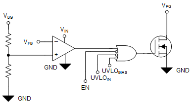
TPS7A52-Q1 ai_pg_circuit_sbvs291.gifFigure 42. Simplified PG Circuit