SBVS304B June 2017 – October 2021 TPS7A83A
PRODUCTION DATA
- 1 Features
- 2 Applications
- 3 Description
- 4 Revision History
- 5 Description (continued)
- 6 Pin Configuration and Functions
-
7 Specifications
- 7.1 Absolute Maximum Ratings
- 7.2 ESD Ratings
- 7.3 Recommended Operating Conditions
- 7.4 Thermal Information
- 7.5 Electrical Characteristics: General
- 7.6 Electrical Characteristics: TPS7A8300A
- 7.7 Electrical Characteristics: TPS7A8301A
- 7.8 Typical Characteristics: TPS7A8300A
- 7.9 Typical Characteristics: TPS7A8301A
- 8 Detailed Description
-
9 Application and Implementation
- 9.1
Application Information
- 9.1.1
External Component Selection
- 9.1.1.1 Adjustable Operation
- 9.1.1.2 ANY-OUT Programmable Output Voltage
- 9.1.1.3 ANY-OUT Operation
- 9.1.1.4 Increasing ANY-OUT Resolution for LILO Conditions
- 9.1.1.5 Recommended Capacitor Types
- 9.1.1.6 Input and Output Capacitor Requirements (CIN and COUT)
- 9.1.1.7 Feed-Forward Capacitor (CFF)
- 9.1.1.8 Noise-Reduction and Soft-Start Capacitor (CNR/SS)
- 9.1.2 Start Up
- 9.1.3 AC and Transient Performance
- 9.1.4 DC Performance
- 9.1.5 Sequencing Requirements
- 9.1.6 Negatively Biased Output
- 9.1.7 Reverse Current
- 9.1.8 Power Dissipation (PD)
- 9.1.1
External Component Selection
- 9.2 Typical Application
- 9.1
Application Information
- 10Power Supply Recommendations
- 11Layout
- 12Device and Documentation Support
- 13Mechanical, Packaging, and Orderable Information
3 Description
The TPS7A83A is a low-noise (4.4 μVRMS), low-dropout, linear regulator (LDO) capable of sourcing 2 A with only 200 mV of maximum dropout. The TPS7A8300A output voltage is pin programmable from 0.8 V to 3.95 V with a 50-mV resolution, and adjustable from 0.8 V to 5.2 V using an external resistor divider. The TPS7A8301A output voltage is pin programmable from 0.5 V to 2.075 V with a 25-mV resolution, and adjustable from 0.5 V to 5.2 V using an external resistor divider.
The combination of low noise , high PSRR, and high output current capability makes the TPS7A83A an excellent choice to power noise-sensitive components such as those found in high-speed communications, video, medical, or test and measurement applications. This device is designed for powering high-performance serializer and deserializer (SerDes), analog-to-digital converters (ADCs), digital-to-analog converters (DACs), and RF components because the high performance of the TPS7A83A limits power-supply-generated phase noise and clock jitter. Specifically, RF amplifiers benefit from the high-performance and 5.2-V output capability of the device.
| PART NUMBER | PACKAGE | BODY SIZE (nom) |
|---|---|---|
| TPS7A83A | VQFN (20) | 3.50 mm × 3.50 mm |
| 5.00 mm × 5.00 mm |
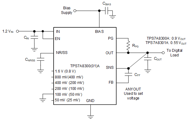
 Typical Application
Circuit