SBVS314B March   2018  – October 2018 TPS7A10

PRODUCTION DATA.  

  1. Features
  2. Applications
  3. Description
    1.     Device Images
      1.      Dropout vs IOUT and Temperature, YKA Package
      2.      Typical Application Circuit
  4. Revision History
  5. Pin Configuration and Functions
    1.     Pin Functions
  6. Specifications
    1. 6.1 Absolute Maximum Ratings
    2. 6.2 ESD Ratings
    3. 6.3 Recommended Operating Conditions
    4. 6.4 Thermal Information
    5. 6.5 Electrical Characteristics
    6. 6.6 Typical Characteristics
  7. Detailed Description
    1. 7.1 Overview
    2. 7.2 Functional Block Diagram
    3. 7.3 Feature Description
      1. 7.3.1 Excellent Transient Response
      2. 7.3.2 Global Undervoltage Lockout (UVLO)
      3. 7.3.3 Active Discharge
      4. 7.3.4 Enable
      5. 7.3.5 Sequencing Requirement
      6. 7.3.6 Internal Foldback Current Limit
      7. 7.3.7 Thermal Shutdown
    4. 7.4 Device Functional Modes
      1. 7.4.1 Normal Mode
      2. 7.4.2 Dropout Mode
      3. 7.4.3 Disable Mode
  8. Application and Implementation
    1. 8.1 Application Information
      1. 8.1.1 Recommended Capacitor Types
      2. 8.1.2 Input and Output Capacitor Requirements
      3. 8.1.3 Load Transient Response
      4. 8.1.4 Dropout Voltage
      5. 8.1.5 Behavior During Transition From Dropout Into Regulation
      6. 8.1.6 Undervoltage Lockout Circuit Operation
      7. 8.1.7 Power Dissipation (PD)
        1. 8.1.7.1 Estimating Junction Temperature
        2. 8.1.7.2 Recommended Area for Continuous Operation
    2. 8.2 Typical Application
      1. 8.2.1 Design Requirements
      2. 8.2.2 Detailed Design Procedure
        1. 8.2.2.1 Input Current
        2. 8.2.2.2 Thermal Dissipation
      3. 8.2.3 Application Curve
  9. Power Supply Recommendations
  10. 10Layout
    1. 10.1 Layout Guidelines
    2. 10.2 Layout Examples
  11. 11Device and Documentation Support
    1. 11.1 Device Support
      1. 11.1.1 Development Support
        1. 11.1.1.1 Evaluation Module
        2. 11.1.1.2 Spice Model
      2. 11.1.2 Device Nomenclature
    2. 11.2 Documentation Support
      1. 11.2.1 Related Documentation
    3. 11.3 Receiving Notification of Documentation Updates
    4. 11.4 Community Resources
    5. 11.5 Trademarks
    6. 11.6 Electrostatic Discharge Caution
    7. 11.7 Glossary
  12. 12Mechanical, Packaging, and Orderable Information

Global Undervoltage Lockout (UVLO)

The TPS7A10 uses two undervoltage lockout (UVLO) circuits: one on the BIAS pin and one on the IN pin to prevent the device from turning on before both VBIAS and VIN rise above their lockout voltages. The two UVLO signals are connected internally through an AND gate, as shown in Figure 38. This internal connection allows the device to be turned off when either rail is below its lockout voltage.
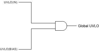
TPS7A10 sbvs314-global-uvlo-1.gif
Figure 38. Global UVLO circuit