SBVS360A February   2020  – November 2020 TPS7B85-Q1

PRODUCTION DATA  

  1. Features
  2. Applications
  3. Description
  4. Revision History
  5. Pin Configuration and Functions
  6. Specifications
    1. 6.1 Absolute Maximum Ratings
    2. 6.2 ESD Ratings
    3. 6.3 Recommended Operating Conditions
    4. 6.4 Thermal Information
    5. 6.5 Electrical Characteristics
    6. 6.6 Switching Characteristics
    7. 6.7 Typical Characteristics
  7. Detailed Description
    1. 7.1 Overview
    2. 7.2 Functional Block Diagram
    3. 7.3 Feature Description
      1. 7.3.1 Enable (EN)
      2. 7.3.2 Power-Good (PG)
        1. 7.3.2.1 Adjustable Power-Good (PGADJ)
      3. 7.3.3 Adjustable Power-Good Delay Timer (DELAY)
      4. 7.3.4 Sense Comparator
      5. 7.3.5 Undervoltage Lockout
      6. 7.3.6 Thermal Shutdown
      7. 7.3.7 Current Limit
    4. 7.4 Device Functional Modes
      1. 7.4.1 Device Functional Mode Comparison
      2. 7.4.2 Normal Operation
      3. 7.4.3 Dropout Operation
      4. 7.4.4 Disabled
  8. Application and Implementation
    1. 8.1 Application Information
      1. 8.1.1 Input and Output Capacitor Selection
      2. 8.1.2 Dropout Voltage
      3. 8.1.3 Reverse Current
      4. 8.1.4 Power Dissipation (PD)
        1. 8.1.4.1 Thermal Performance Versus Copper Area
      5. 8.1.5 Estimating Junction Temperature
      6. 8.1.6 SI Pin
        1. 8.1.6.1 Calculating the Sense Input (SI) Pin Threshold
        2. 8.1.6.2 Different Uses for the Sense Input Pin
          1. 8.1.6.2.1 Monitoring Input Voltage
          2. 8.1.6.2.2 Creating OV and UV Power-Good
          3. 8.1.6.2.3 Monitoring a Separate Supply Voltage
      7. 8.1.7 Pulling Up the SO and PG Pins to a Different Voltage
      8. 8.1.8 Power-Good
        1. 8.1.8.1 Setting the Adjustable Power-Good Threshold
        2. 8.1.8.2 Setting the Adjustable Power-Good Delay
    2. 8.2 Typical Application
      1. 8.2.1 Design Requirements
      2. 8.2.2 Detailed Design Procedure
        1. 8.2.2.1 Input Capacitor
        2. 8.2.2.2 Output Capacitor
      3. 8.2.3 Application Curves
  9. Power Supply Recommendations
  10. 10Layout
    1. 10.1 Layout Guidelines
      1. 10.1.1 Package Mounting
      2. 10.1.2 Board Layout Recommendations to Improve PSRR and Noise Performance
    2. 10.2 Layout Example
  11. 11Device and Documentation Support
    1. 11.1 Device Support
      1. 11.1.1 Device Nomenclature
    2. 11.2 Receiving Notification of Documentation Updates
    3. 11.3 Support Resources
    4. 11.4 Trademarks
    5. 11.5 Electrostatic Discharge Caution
    6. 11.6 Glossary

Pulling Up the SO and PG Pins to a Different Voltage

Because the sense out (SO) and power-good (PG) pins are pulled up internally to the output rail, they cannot be pulled up to any voltage or wire AND'd like a typical open-drain PG output can be. If these signals must be pulled up to another logic level then an external circuit can be implemented using a PMOS transistor and a pullup resistor. Implementing the circuit shown in Figure 8-10 allows the outputs to be pulled up to any logic rail. This implementation also allows the outputs to be AND'd together like the traditional power-good pins.
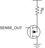
GUID-60ECAE97-F52D-42D4-9850-B8BCB741AFE7-low.gifFigure 8-10 Additional Components for the SO and PG Pins to be Pulled Up to Another Rail