SBVS451 August 2024 TPS7A20C
PRODUCTION DATA
- 1
- 1 Features
- 2 Applications
- 3 Description
- 4 Pin Configuration and Functions
- 5 Specifications
- 6 Detailed Description
- 7 Application and Implementation
- 8 Device and Documentation Support
- 9 Revision History
- 10Mechanical, Packaging, and Orderable Information
7.1.5.2 Recommended Area for Continuous Operation
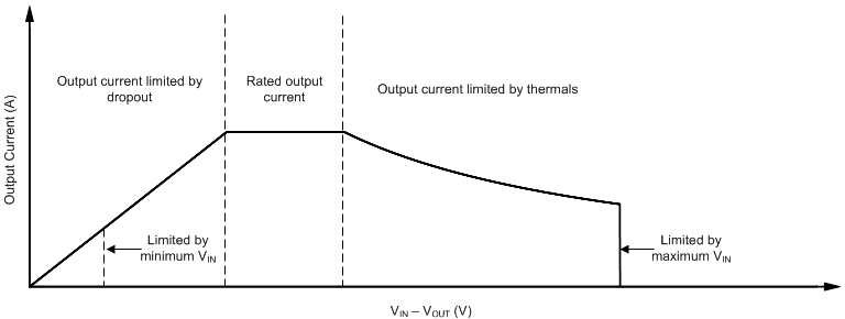
The operational area of an LDO is limited by the dropout voltage, output current, junction temperature, and input voltage. The recommended area for continuous operation for a linear regulator is given in Figure 7-3 and is separated into the following parts:
- Dropout voltage limits the minimum differential voltage between the input and the output (VIN – VOUT) at a given output current level. See the Dropout Operation section for more details.
- The rated output currents limits the maximum recommended output current level. Exceeding this rating causes the device to fall out of specification.
- The rated junction temperature limits
the maximum junction temperature of the device. Exceeding this rating causes the device
to fall out of specification and reduces long-term reliability.
- The shape of the slope is given by Equation 4. The slope is nonlinear because the maximum-rated junction temperature of the LDO is controlled by the power dissipation across the LDO. Thus, when VIN – VOUT increases the output current decreases.
- The rated input voltage range governs both the minimum and maximum of VIN – VOUT.
Figure 7-3 shows the recommended area of operation for this device on a JEDEC-standard high-K board with a RθJA, as given in the Thermal Information table.
 Figure 7-3 Region
Description of Continuous Operation Regime