SBVS451 August 2024 TPS7A20C
PRODUCTION DATA
- 1
- 1 Features
- 2 Applications
- 3 Description
- 4 Pin Configuration and Functions
- 5 Specifications
- 6 Detailed Description
- 7 Application and Implementation
- 8 Device and Documentation Support
- 9 Revision History
- 10Mechanical, Packaging, and Orderable Information
7.1.3 Load Transient Response
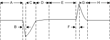
The load-step transient response is the output voltage response by the LDO to a step in load current, whereby output voltage regulation is maintained. There are two key transitions during a load transient response: from a light to a heavy load and from a heavy to a light load. The regions shown in Figure 7-1 are broken down as follows. Regions A, E, and H are where the output voltage is in steady-state.
 Figure 7-1 Load Transient Waveform
During transitions from a light load to a heavy load, the:
- Initial voltage dip is a result of the depletion of the output capacitor charge and parasitic impedance to the output capacitor (region B)
- Recovery from the dip results from the LDO increasing the sourcing current, and leads to output voltage regulation (region C)
During transitions from a heavy load to a light load, the:
- Initial voltage rise results from the LDO sourcing a large current, and leads to the output capacitor charge to increase (region F)
- Recovery from the rise results from the LDO decreasing the sourcing current in combination with the load discharging the output capacitor (region G)
A larger output capacitance reduces the peaks during a load transient but slows down the response time of the device. A larger DC load also reduces the peaks. The amplitude of the transition is lowered and a higher current discharge path is provided for the output capacitor.
This LDO is designed to provide best transient response performance when the load current is limited to approximately 200mA or less.