SBVU070B September   2021  – August 2022 TPS7A94


  1.   Abstract
  2.   Trademarks
  3. 1Introduction
    1. 1.1 Before You Begin
  4. 2EVM Setup
    1. 2.1 Inputs/Outputs Connectors and Jumper Descriptions
      1. 2.1.1  J1 – IN
      2. 2.1.2  J2 – OUT
      3. 2.1.3  J3
      4. 2.1.4  TP1 – IN
      5. 2.1.5  TP2 – PG
      6. 2.1.6  TP3 – SNS
      7. 2.1.7  TP4 – PG_FB
      8. 2.1.8  TP5 – OUT
      9. 2.1.9  TP6 – EN
      10. 2.1.10 TP7 – GND
      11. 2.1.11 TP8 – GND
    2. 2.2 Soldering Guidelines
    3. 2.3 Equipment Connections
  5. 3Operation
  6. 4PCB Layout
  7. 5Schematic
  8. 6Bill of Materials
  9. 7Revision History

PCB Layout

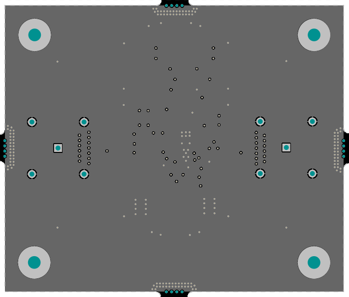
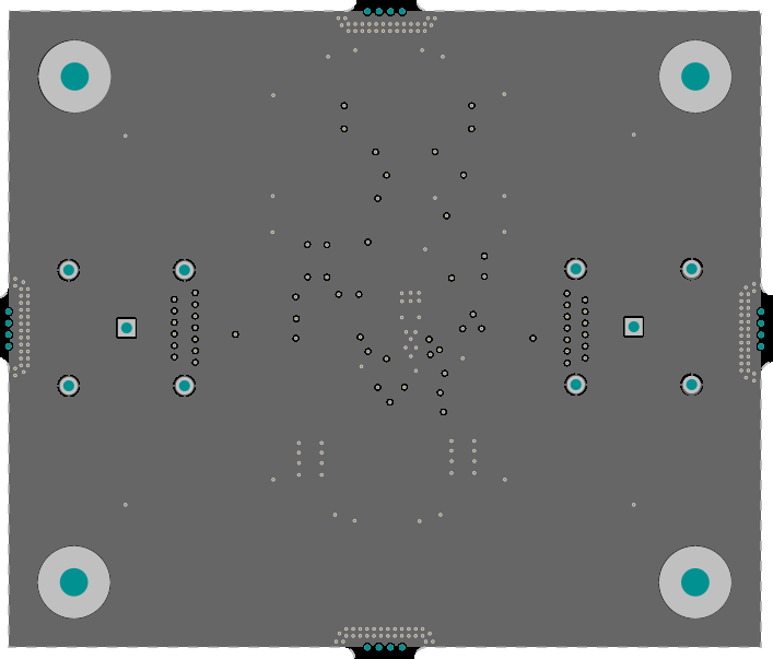
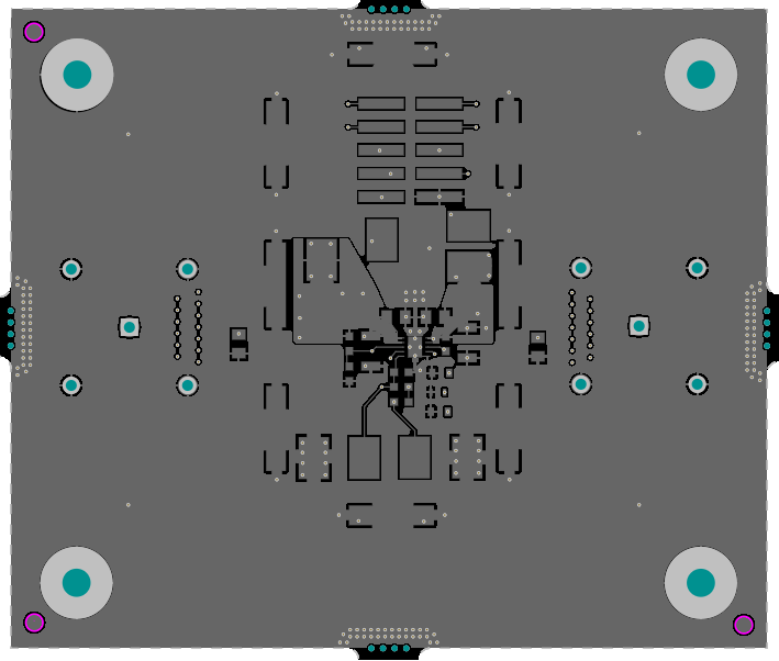
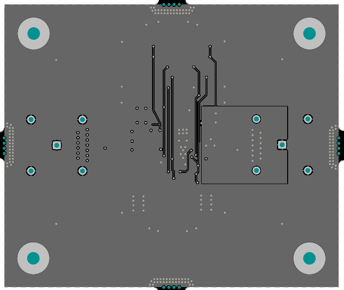
Figure 4-1 to Figure 4-5 illustrate the PCB layout for this EVM.
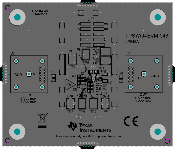
GUID-20210909-SS0I-JCWS-0919-B8RJ9RFSGHDX-low.pngFigure 4-1 Assembly Layer
GUID-20210909-SS0I-PQNV-JSXF-VCBTMGH8WF2S-low.pngFigure 4-3 First Middle Layer
GUID-20210909-SS0I-2HZ7-9PGV-LLVTZ0BD9RZM-low.pngFigure 4-5 Bottom Layer Routing
GUID-20210909-SS0I-DSKP-D90W-4DDTNTWN4LDS-low.pngFigure 4-2 Top Layer Routing
GUID-20210909-SS0I-QTT4-NK3X-6PGL3M0NBSKS-low.pngFigure 4-4 Second Middle Layer