SBVU074 November 2021
3.3 TPS7A13 LDO Operation
The TPS7A13EVM-057 evaluation module contains the TPS7A13 LDO with input, bias, and output capacitors installed. These four components provide the minimum required solution size, as illustrated by the white boxes in Figure 3-2. Additional pads are available to test the LDO with additional input and output capacitors beyond what is already installed on the EVM. The TPS7A13 LDO can be enabled or disabled by using the J7 3-pin header.
- Place a 2-pin shunt across the header to tie VIN to EN to enable the device.
- Place a 2-pin shunt across the header to tie GND to EN to disable the device.
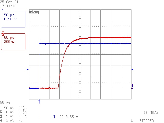
Alternatively, by connecting an external function generator to TP1 (EN) and a nearby GND post (J11), the user can enable or disable the TPS7A13 LDO after VIN is applied. Figure 3-1 shows the result of the TPS7A13EVM-057 during turn on. The blue trace is the enable voltage, and the red trace is the output voltage.
 Figure 3-1 TPS7A13EVM-057 Turn
On
Figure 3-1 TPS7A13EVM-057 Turn
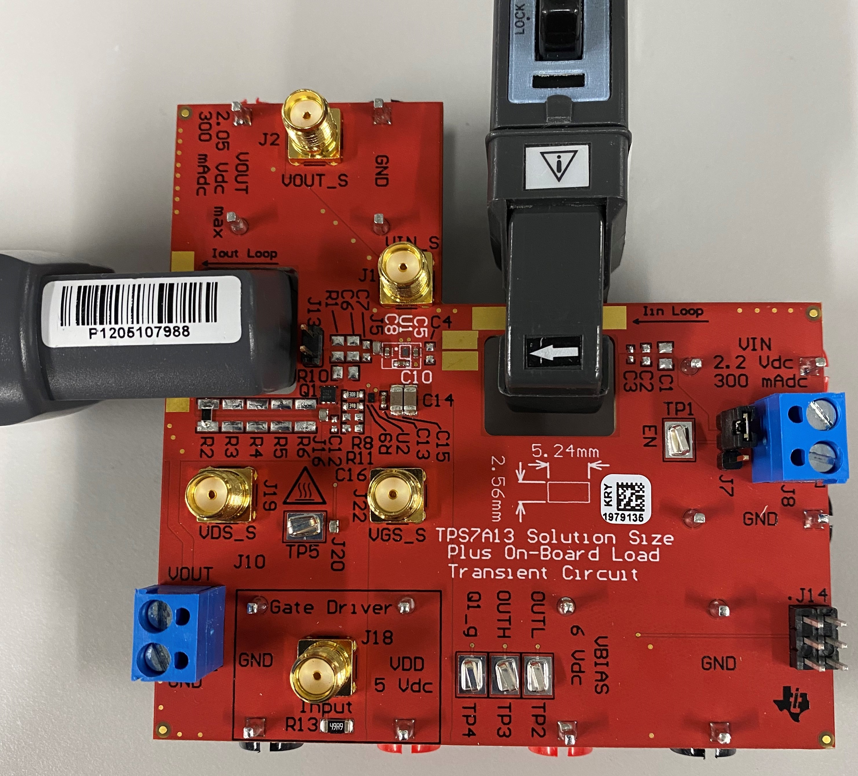
OnIf desired, a current probe can be inserted in the EVM as shown in Figure 3-2 to measure the input and output current. The slots were sized to fit most current probes, such as the LeCroy™ AP015 or CP031 current probes.
 Figure 3-2 TPS7A13EVM-057 With Current
Probes Attached
Figure 3-2 TPS7A13EVM-057 With Current
Probes AttachedThe user has two options for providing a DC load on the output of the TPS7A13. J10 can be used to place a DC load that flows through the current sense path on the output of the LDO. Alternatively, the J4 (VOUT) and J12 (GND) banana connectors can be used for external measurements and loading; however, the IOUT loop does not sense current flowing through these connectors. In cases where very fast transient tests are performed, ringing may be observed on VIN or VOUT as a result of the parasitic inductance within the PCB of the EVM. A strip of wire placed on the exposed copper in the current path can reduce this ringing. Select the correct size of additional wire to fill the volume of the current probe. For most current probes, a 10 AWG wire can be used.
Optional kelvin sense points are provided using the SMA connectors J1 (VIN) and J2 (VOUT).