SCAA145 August 2024 SN74AC244 , SN74AC244-Q1 , SN74AC245 , SN74AC245-Q1
Introduction
The AC logic family provides some of the fastest and highest drive strength single-ended logic buffers on the market today. Along with high speeds and heavy loading comes large temperature increases. In this document, we show through examples how to utilize the provided thermal metrics to determine application specific limitations.
There are many different electronic products with specific use-cases of medium to high speed digital signal driving requirements. Pulse width modulation (PWM) is common in motor speed control, power regulation, LED control, and audio amplification. PWM signals are created by alternating between digital high state (ON) and low state (OFF) signals. These signals can be changed by varying pulse width (duration of the high state signal), increasing or decreasing duty cycle, as well as increasing or decreasing frequency. Digital buffers can be used to redrive PWM signals for a variety of applications across a wide range of frequencies and duty cycles.
 Figure 1 Rack servers
 Figure 2 Printed circuit board
traces
Figure 2 Printed circuit board
tracesRack servers commonly have controlled imepdance traces that require strong drivers. The AC logic family supports direct drive of 50Ω traces and can support relatively high speeds and heavy loads. Generally speaking, traces under 12cm add capacitance without creating transmission line effects, and traces over 12cm require controlled impedance and correct terminations to mitigate transmisison line effects. Source termination to match impedance of the transmission line is all that is required for an AC driver like the SN74AC244 to be used for this type of application. See Design Considerations for Logic Products for details.
Low voltage relays are common in test and measurement as well as other industrial applications. The high drive strength and integrated output clamp diodes of the AC logic family allow for direct drive of low voltage relays. These relays are often used to control higher amperage loads like servo motors, audio amplifiers, and temperature sensors. Low voltage relays can be actuated with 5V and up to 30mA of current. Microcontrollers, FPGAs, and CPUs seldom have the level of drive strength required to drive these directly. The SN74AC244 is capable of driving all eight channels with 24mA each making the SN74AC244 an excellent choice for this application and enabling the use of these relays within a system.
Power Calculation
Temperature increases are caused by power consumption in a semiconductor device. To accurately calculate power consumption for a CMOS logic gate, we must define a few terms and equations.
In Equation 1 we have the total power (PTOTAL), static power (PS), transient power (PT), capacitive load power (PLC), negative resistive load power (PLRN), and positive resistive load power (PLRP). The load power values (PLC, PLRN, and PLRP) are specifically the power consumed within the CMOS logic device to drive these loads. The power consumption equation components PS, PLRN, and PLRP can be considered as a constant power draw, with no variation due to operating frequency, while the components PT and PLC are both frequency dependent.
In Equation 2 we have the transient power consumption (PT), power dissipation capacitance (Cpd), supply voltage (VCC), input frequency (fi), and number of channels switching, (NSW). This equation assumes that all channels are switching at the same frequency and have the same power dissipation capacitance value.
In Equation 3 we have the capacitive load power dissipation (PLC), supply voltage (VCC), capacitive load (CL), output frequency (fo), and number of channels switching (NSW).
In Equation 4 we have the static power consumption (PS), supply voltage (VCC), and static supply current (ICC).
In Equation 5 we have the negative resistive load power dissipation (PLRN), output duty cycle (Do), supply voltage (VCC), output high-state voltage (VOH), and output pull-down resistance (RPD).
In Equation 6 we have the positive resistive load power dissipation (PLRP), output duty cycle (Do), supply voltage (VCC), output high-state voltage (VOH), and output pull-up resistance (RPU).
The resistive and static power consumption values can often be ignored when doing thermal calculations for CMOS logic gates, as these values do not generally have a large impact on the total power consumption. For the sake completeness, these calculations are included in this document, but in the following examples you can see how these values are generally unnecessary for thermal dissipation calculations.
The following sections provide calculated and bench-verified thermal performance for the SN74AC244 device in common applications.
Application 1: Calculations
The SN74AC244 provides eight independent buffers. In this application, we tie together all eight inputs to a single 10MHz, 50% duty cycle clock source and drive independent loads with each output. Using shared clock inputs to split into multiple outputs is known as a clock fanout application.
The output loading is equivalent to approximately 10 CMOS device inputs, with a total capacitive load (CL) of 56pF per channel and total resistive load of 500kΩ (RLP and RLN) per channel. CL is the closes value to 50pF that was available locally at the time of testing. RLP and RLN values were calculated based on the supply voltage, 5V, and an assumed input leakage current maximum of 1µA per input. With 10 parallel inputs, this is 10µA maximum at 5V, which is equivalent to 500kΩ.
First, we calculate the static power consumption numbers. Before plugging values into the given equations, we need to determine the VOH and VOL values for this loading. The data sheet provides the worst-case 4.5V supply VOH at 50µA load as VCC – 0.1V, and VOL at the same load as 0.1V. Our loading is ten times less, so the voltage is also scaled to be ten times less, resulting in VCC-VOH = 0.01V, and VOL = 0.01V.
The total power consumption for all static sources is less than 1mW in this application. Rounding to 1mW and selecting the worst-case package selection for power dissipation, PW (TSSOP), we can calculate the temperature rise from this power consumption (1mW) and the given RθJA of 126.2°C/W given in the data sheet. The power consumption of 1mW and related thermal resistance value result in a temperature rise of less than 0.13°C, or in other words, a negligible amount. To be clear, the above calculations are not necessary for normal applications due to the small impact of those power values, but are included here for completeness and to demonstrate the reason static power consumption can be ignored in most applications for CMOS logic devices.
Moving on to the dynamic power dissipation, there is more power consumption. The Cpd value is taken from the data sheet as 45pF.
Together, these two values give 202mW, which is a considerable amount of power consumption. Given these numbers, the device has a temperature increase in the PW package of approximately 25.5C (0.202W × 126.2°C/W = 25.49°C).
Given that the junction temperature has a maximum of 150°C and the device has an ambient operating temperature maximum of 125°C, the SN74AC244 is capable of running at this power level across almost all of the entire ambient operating temperature range. At the high end, the device is limited to 124.5°C to avoid exceeding the maximum junction temperature of 150°C.
Repeating the above calculations for the DGS package (RθJA = 123.5°C/W), provides a temperature increase of 24.9°C, resulting in TJ(max) of 149.9°C. The temperature increase indicates slightly better thermal performance of the DGS package, and the ability to use the device across the full temperature range in this application.
Application 1: Bench testing
In our experiments, we can only measure the case temperature of the device, and thus the junction temperature must be calculated from the experimental data. The PCBs used for this experiment are from the 14-24-LOGIC-EVM. These boards are not optimized for thermal conductivity per the application report Semiconductor and IC Package Thermal Metrics, but do represent a typical two-layer board design.
From the application report Semiconductor and IC Package Thermal Metrics, "RθJA is a variable function of not just the package, but of many other system level characteristics such as the design and layout of the printed circuit board (PCB) on which the part is mounted. In effect, the test board is a heat sink that is soldered to the leads of the device. Changing the design or configuration of the test board changes the efficiency of the heat sink and therefore the measured RθJA."
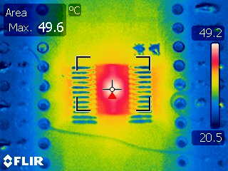
 Figure 3 Thermal image of PW package operating at 10MHz, 5V supply, 8 channels
switching with 56pF load each
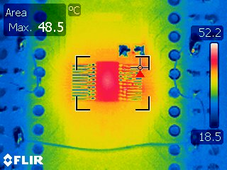
 Figure 4 Thermal image of DGS package operating at 10MHz, 5V supply, 8 channels
switching with 56pF load each
Figure 4 Thermal image of DGS package operating at 10MHz, 5V supply, 8 channels
switching with 56pF load eachThe operating junction temperature can be calculated from the measured case temperature using Equation 14. The temperature of each package was measured under the previously calculated conditions (TA = 25°C, VCC = 5V, fin = 10MHz, CL = 56pF, RP = RL = 500kΩ) and the values are provided in Table 1. The total calculated power consumption is 202mW for each case.
| Measured Case Temperature (°C) | ΨJT (°C/W) | Calculated Junction Temp | Calculated Temperature Increase | Data sheet Specified RθJA | Calculated Application Specific RθJA | |
| PW | 49.6 | 22.3 | 53.8 | 28.8 | 126.2 | 151.8 |
| DGS | 48.5 | 7.8 | 50.0 | 25 | 123.5 | 131.5 |
There is a large discrepancy between the data sheet provided RθJA and the application specific RθJA for the PW package as calculated from this experiment. The discrepancy between data sheet calculated thermal resistance values and experimentally derived values is explained in detail in the application report Semiconductor and IC Package Thermal Metrics, however we can restate briefly here that the PCB design has an enormous impact on the thermal performance of a device, and this PCB is not optimized for thermal performance.
The core take-away from this experiment is that the DGS package provides significant space savings while also providing improved thermal conductivity. Additionally, the calculated temperature increase of 25.5°C based on the data sheet thermal specifications is close to the experimentally derived values of 28.8C and 25C, providing confirmation that calculated values are a valid method for thermal performance prior to board construction, even with non-ideal PCB design.
Application 2: Calculations
In this application, we again utilize the SN74AC244 and use the same conditions as those described in Application 1: Calculations. The difference from Application 1 is the package and PCB. In this application, we utilize the RKS (WQFN) package and test one PCB with the thermal pad floating, and another PCB with the thermal pad connected to a ground plane per the data sheet recommendations.
See Application 1: Calculations for details, as the loading and power dissipation calculations are the same for this application.
The previously calculated power consumption was 202mW for this application. In the RKS package (RθJA = 67.7°C/W), the SN74AC244 has an expected temperature increase of approximately 13.7°C (0.202W × 67.7°C/W = 13.67°C) resulting in a junction temperature of 38.7°C at TA = 25°C.
Given that the junction temperature has a maximum of 150°C and the device has an ambient operating temperature maximum of 125°C, the SN74AC244 is capable of continuously running at this power level across the entire ambient operating temperature range based on the calculated temperature increase.
Application 2: Bench testing
In our experiments, we can only measure the case temperature of the device, and thus the junction temperature must be calculated from the experimental data. One PCB used for this experiment was from the 14-24-LOGIC-EVM, while the other was a modified version to include vias connecting the thermal pad to ground while maintaining all other board features, stackup, and geometry. These boards are not optimized for thermal conductivity per the application report Semiconductor and IC Package Thermal Metrics, but do represent a typical two-layer board design.
From the application report Semiconductor and IC Package Thermal Metrics, "RθJA is a variable function of not just the package, but of many other system level characteristics such as the design and layout of the printed circuit board (PCB) on which the part is mounted. In effect, the test board is a heat sink that is soldered to the leads of the device. Changing the design or configuration of the test board changes the efficiency of the heat sink and therefore the measured RθJA."
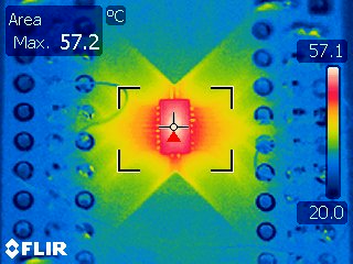
 Figure 5 Thermal image of RKS
package operating at 10MHz, 5V supply, 8 channels switching with 56pF load
each with a floating thermal pad connection
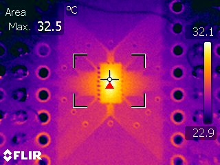
 Figure 6 Thermal image of RKS
package operating at 10MHz, 5V supply, 8 channels switching with 56pF load
each with the thermal pad connected to a ground plane
Figure 6 Thermal image of RKS
package operating at 10MHz, 5V supply, 8 channels switching with 56pF load
each with the thermal pad connected to a ground planeThe operating junction temperature can be calculated from the measured case temperature using Equation 14. The temperature of each package was measured under the previously calculated conditions (TA = 25°C, VCC = 5V, fin = 10MHz, CL = 56pF, RP = RL = 500kΩ) and the values are provided in Table 1. The total calculated power consumption is 202mW for each case.
| Measured Case Temperature (°C) | ΨJT (°C/W) | Calculated Junction Temp (°C) | Calculated(1) Temperature Increase (°C) | Data sheet Specified RθJA (°C/W) | Calculated(2) Application Specific RθJA (°C/W) | |
| RKS with floating thermal pad | 57.2 | 10.3 | 59.3 | 34.3 | 67.7 | 169.7 |
| RKS with grounded thermal pad | 32.5 | 10.3 | 34.6 | 9.6 | 67.7 | 47.4 |
As mentioned in the previous application, the PCB design has an enormous impact on the thermal performance of a device. The data provided shows that the thermal performance of the RKS package is drastically improved by connecting the thermal pad to an underlying ground plane per the data sheet recommendations. With good thermal design, the RKS package has excellent thermal characteristics and saves space over other package options.