SCAS288R January 1993 – August 2024 SN54LVC86A , SN74LVC86A
PRODUCTION DATA
- 1
- 1 Features
- 2 Applications
- 3 Description
- 4 Pin Configuration and Functions
-
5 Specifications
- 5.1 Absolute Maximum Ratings
- 5.2 ESD Ratings
- 5.3 Recommended Operating Conditions, SN54LVC86A
- 5.4 Recommended Operating Conditions, SN74LVC86A
- 5.5 Thermal Information
- 5.6 Electrical Characteristics, SN54LVC86A
- 5.7 Electrical Characteristics, SN74LVC86A
- 5.8 Switching Characteristics, SN54LVC86A
- 5.9 Switching Characteristics, SN74LVC86A
- 5.10 Operating Characteristics
- 5.11 Typical Characteristics
- 6 Parameter Measurement Information
- 7 Detailed Description
- 8 Application and Implementation
- 9 Device and Documentation Support
- 10Revision History
- 11Mechanical, Packaging, and Orderable Information
6 Parameter Measurement Information
Phase relationships between waveforms were chosen arbitrarily for the examples listed in the following table. All input pulses are supplied by generators having the following characteristics: PRR ≤ 1MHz, ZO = 50Ω, tt ≤ 2.5ns.
The outputs are measured individually with one input transition per measurement.
| VCC | Vt | RL | CL | ΔV |
|---|---|---|---|---|
| 1.8V ± 0.15V | VCC/2 | 1kΩ | 30pF | 0.15V |
| 2.5V ± 0.2V | VCC/2 | 500Ω | 30pF | 0.15V |
| 2.7V | 1.5V | 500Ω | 50pF | 0.3V |
| 3.3V ± 0.3V | 1.5V | 500Ω | 50pF | 0.3V |

(1) CL includes probe
and test-fixture capacitance.
Figure 6-1 Load Circuit for Push-Pull
Outputs
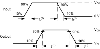
(1) The greater between
tr and tf is the same as tt.
Figure 6-3 Voltage Waveforms, Input
and Output Transition Times
(1) The
greater between tPLH and tPHL is the same as
tpd.
Figure 6-2 Voltage Waveforms
Propagation Delays